Quick Summary:

Researchers developed a new material called High Kinetic Inductance (HKI) that allows for the creation of scalable reversible logic chips at cryogenic temperatures, enabling the replication of complete reversible logic subsystems according to Moore's law.

Summary

Researchers developed about a dozen semiconductor reversible (or adiabatic) logic chips since the early 1990s, validating circuit designs and proving the concept--but scale up required a further advance. This document shows that cryogenic inductors made of a new High Kinetic Inductance (HKI) material provide the advance. This material can be deposited as an integrated circuit layer, where it has enough energy recycling capacity to power a reversible circuit of the same size. This allows a designer to replicate and scale a complete reversible logic subsystem in accordance with Moore's law.

AI Key Findings

Generated Jun 09, 2025

Methodology

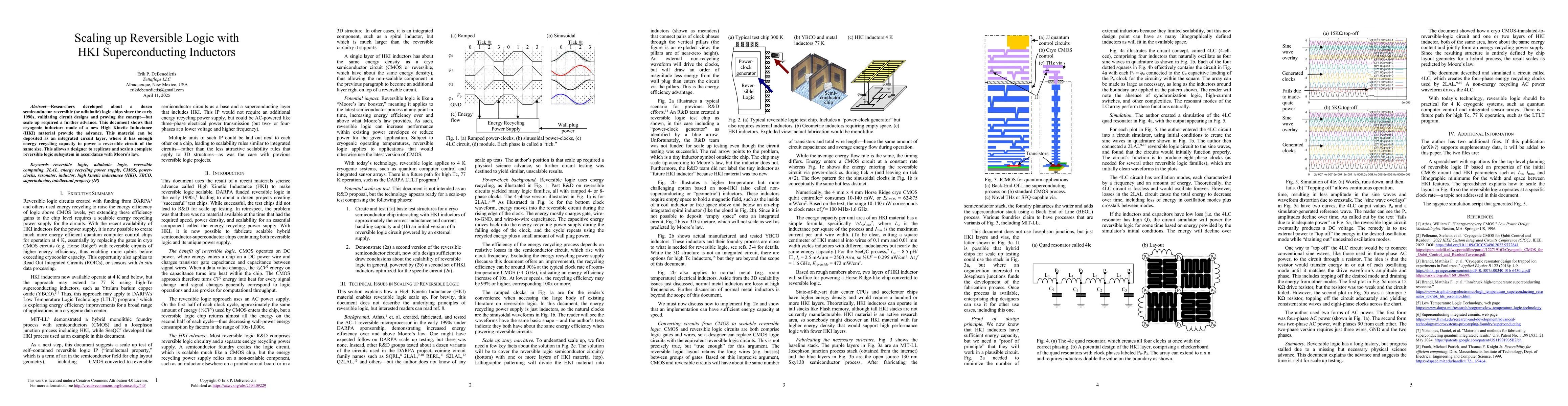
The research proposes using High Kinetic Inductance (HKI) superconducting inductors as an integrated circuit layer to power reversible logic circuits, enabling scaling in accordance with Moore's law.

Key Results

  • HKI material can be deposited as an IC layer with sufficient energy recycling capacity to power reversible circuits of the same size.
  • HKI inductors have energy density comparable to cryogenic semiconductor circuits, allowing them to become an additional layer on top of reversible circuitry.
  • Reversible logic, powered by HKI inductors, can serve as a 'Moore's law booster' by increasing energy efficiency beyond standard CMOS technology.
  • The technology is ready for a scale-up test involving basic test structures and an initial reversible logic circuit powered by HKI inductors.

Significance

This research is significant as it addresses the scalability issue of reversible logic, which has been a barrier to its widespread adoption. By providing a solution for integrating inductors directly onto reversible logic circuits, this work can lead to more energy-efficient computing systems, particularly for cryogenic applications such as quantum computer control and integrated sensor arrays.

Technical Contribution

The introduction of HKI superconducting inductors as an integrated layer for powering reversible logic circuits, enabling scalability and energy efficiency improvements.

Novelty

This work distinguishes itself by presenting a novel method for overcoming the scalability limitations of reversible logic through the use of HKI materials, which can be directly integrated into semiconductor circuits, unlike previous approaches that relied on external, non-scalable inductors.

Limitations

  • The paper does not detail the specifics of fabricating the HKI inductors or the challenges associated with integrating them into existing semiconductor processes.
  • The proposed scale-up test is conceptual and does not provide concrete implementation details or a timeline for execution.

Future Work

  • Further research should focus on developing practical fabrication processes for HKI inductors and integrating them with reversible logic circuits.
  • Experimental validation of the proposed scale-up test phases is necessary to confirm the feasibility and efficiency of the HKI-powered reversible logic approach.

Paper Details

PDF Preview

Download PDF

Key Terms

No key terms available for this paper.

No citations found for this paper.

Comments (0)

This website uses cookies to ensure you get the best experience. Learn more