01
MethodologyHow they did it
Scanning probe microscopy measurements of metallic nanocontacts between controlled electromigration cycles
This study utilizes scanning probe microscopy to image metallic nanocontacts formed via electromigration cycles, achieving a resolution of approximately 3 nm. The nanowires are fabricated through shadow evaporation, and the thinning process reveals that the slit initially follows grain boundaries before splitting them, with current distribution shifting to smaller contacts requiring less power as the slit forms.
This study utilizes scanning probe microscopy to image metallic nanocontacts formed via electromigration cycles, achieving a resolution of approximately 3 nm. The nanowires are fabricated through shadow evaporation, and the thinning process reveals that the slit initially follows grain boundaries before splitting them, with current distribution shifting to smaller contacts requiring less power as the slit forms.
Scanning probe microscopy measurements of metallic nanocontacts between controlled electromigration cycles More in Methodology →
The highest resolution obtained using scanning force microscopy is about 3 nm. — During the first few electromigration cycles, the overall slit structure of the nanocontact is formed. More in Key Results →
Investigating possible transistor functionality of single molecules and studying the structural evolution of nanowires during controlled electromigration More in Significance →
The insulating oxide layer covering the Si substrate complicates scanning tunneling microscopy (STM) studies. — A contamination layer was formed on the sample in STM images due to contact with chemicals during electron beam lithography fabrication More in Limitations →
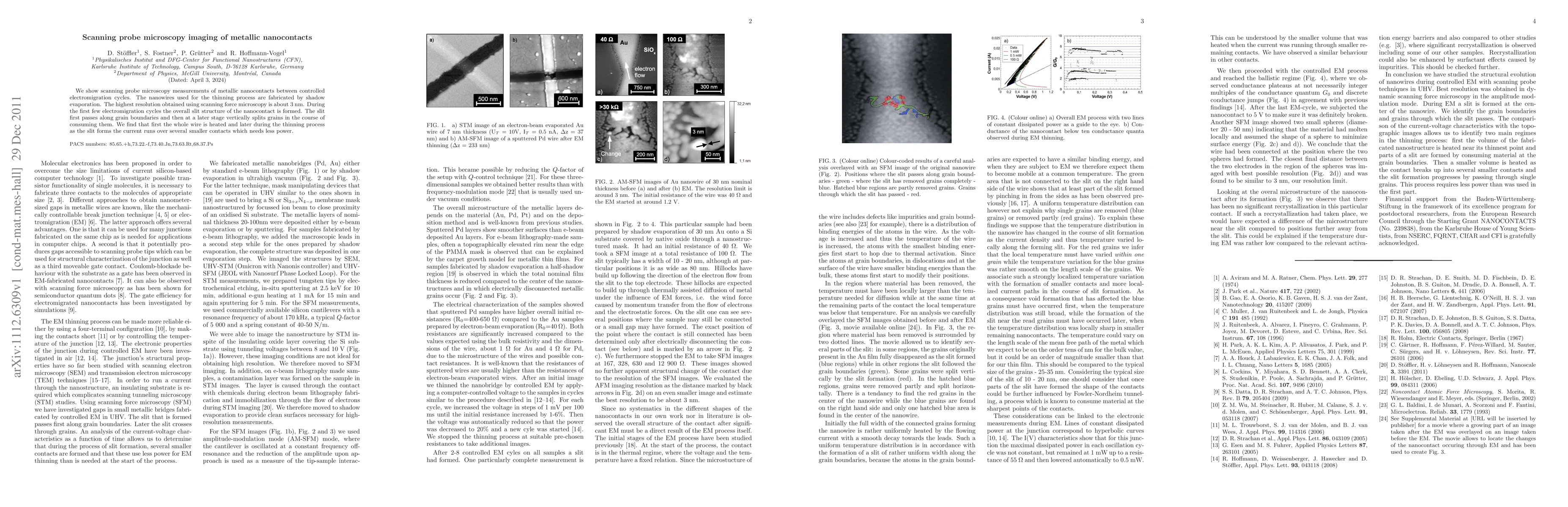
We show scanning probe microscopy measurements of metallic nanocontacts between controlled electromigration cycles. The nanowires used for the thinning process are fabricated by shadow evaporation. The highest resolution obtained using scanning force microscopy is about 3 nm. During the first few electromigration cycles the overall slit structure of the nanocontact is formed. The slit first passes along grain boundaries and then at a later stage vertically splits grains in the course of consuming them. We find that first the whole wire is heated and later during the thinning process as the slit forms the current runs over several smaller contacts which needs less power.
Seven facets of this paper, analysed and brought into focus by AI.
Investigating possible transistor functionality of single molecules and studying the structural evolution of nanowires during controlled electromigration
Scanning probe microscopy measurements of metallic nanocontacts between controlled electromigration cycles
Investigating possible transistor functionality of single molecules and studying the structural evolution of nanowires during controlled electromigration
Scanning probe microscopy imaging of metallic nanocontacts between controlled electromigration cycles
The formation of smaller contacts during electromigration, which requires less power than initially needed
Current paper (gray), citations (green), references (blue)
Display is limited for performance on very large graphs.
Discussion 0