Scanning quantum vortex microscopy reveals thickness-dependent pinning nano-network in superconducting Nb-films
Publication
Metrics
AI Quick Summary
This study utilizes scanning quantum vortex microscopy to map the pinning forces of quantum vortices in Nb-films of varying thicknesses, revealing a thickness-dependent granular pinning network linked to the films' microstructure. The technique can be extended to other type II superconducting materials.
Paper Preview
Abstract
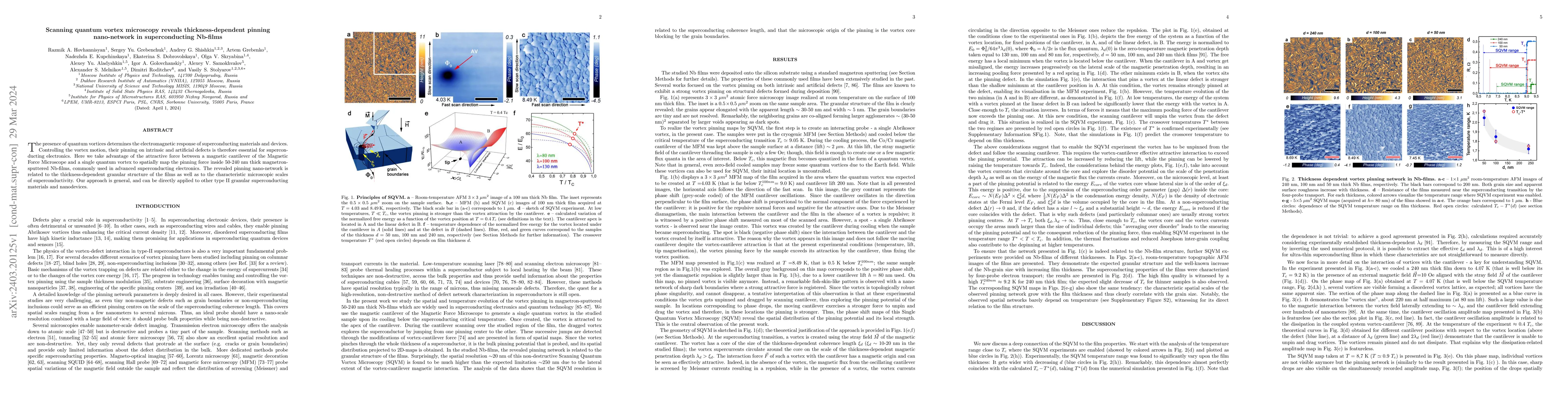
The presence of quantum vortices determines the electromagnetic response of superconducting materials and devices. Controlling the vortex motion, their pinning on intrinsic and artificial defects is therefore essential for superconducting electronics. Here we take advantage of the attractive force between a magnetic cantilever of the Magnetic Force Microscope and a single quantum vortex to spatially map the pinning force inside 50-240 nm thick magnetron-sputtered Nb-films, commonly used in advanced superconducting electronics. The revealed pinning nano-network is related to the thickness-dependent granular structure of the films as well as to the characteristic microscopic scales of superconductivity. Our approach is general, and can be directly applied to other type II granular superconducting materials and nanodevices.
AI Key Findings
Get AI-generated insights about this paper's methodology, results, significance, and more — seven facets brought into focus.
Impact
Paper Details
Authors
PDF Preview
Key Terms
Citation Network
Current paper (gray), citations (green), references (blue)
Display is limited for performance on very large graphs.
Discussion 0