Scanning Transmission Electron Microscopy of Oxide Interfaces and Heterostructures
Publication
Metrics
AI Quick Summary
This paper discusses the application of scanning transmission electron microscopy (STEM) for characterizing thin film oxide interfaces and heterostructures, emphasizing its high-resolution capabilities to resolve structure, chemistry, and defects, which are crucial for refining growth processes and achieving desired material properties.
Paper Preview
Abstract
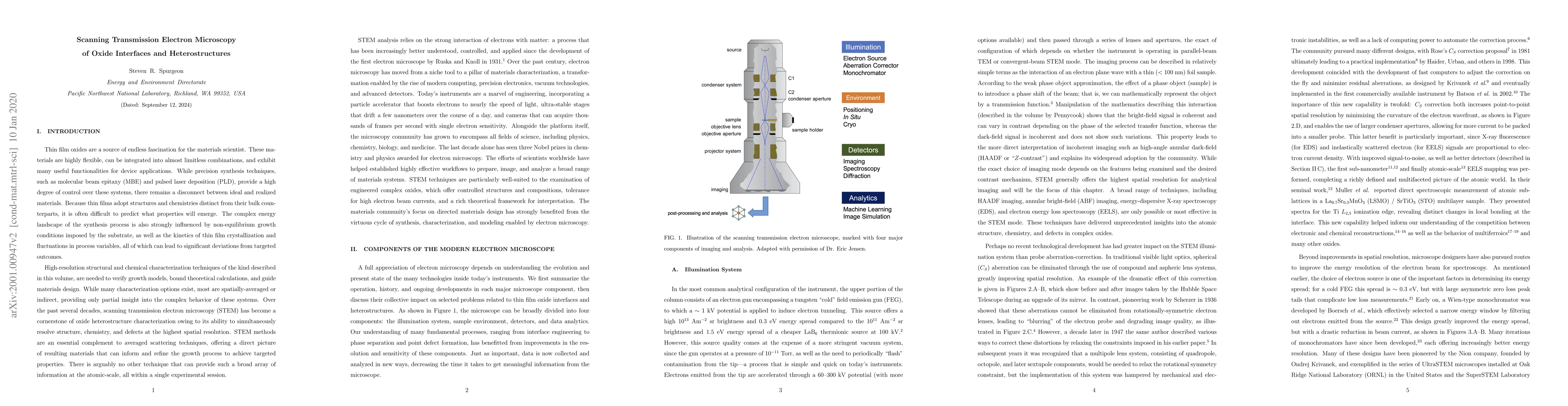
Thin film oxides are a source of endless fascination for the materials scientist. These materials are highly flexible, can be integrated into almost limitless combinations, and exhibit many useful functionalities for device applications. While precision synthesis techniques, such as molecular beam epitaxy (MBE) and pulsed laser deposition (PLD), provide a high degree of control over these systems, there remains a disconnect between ideal and realized materials. Because thin films adopt structures and chemistries distinct from their bulk counterparts, it is often difficult to predict what properties will emerge. The complex energy landscape of the synthesis process is also strongly influenced by non-equilibrium growth conditions imposed by the substrate, as well as the kinetics of thin film crystallization and fluctuations in process variables, all of which can lead to significant deviations from targeted outcomes. High-resolution structural and chemical characterization techniques, as described in this volume, are needed to verify growth models, bound theoretical calculations, and guide materials design. While many characterization options exist, most are spatially-averaged or indirect, providing only partial insight into the complex behavior of these systems. Over the past several decades, scanning transmission electron microscopy (STEM) has become a cornerstone of oxide heterostructure characterization owing to its ability to simultaneously resolve structure, chemistry, and defects at the highest spatial resolution. STEM methods are an essential complement to averaged scattering techniques, offering a direct picture of resulting materials that can inform and refine the growth process to achieve targeted properties. There is arguably no other technique that can provide such a broad array of information at the atomic-scale, all within a single experimental session.
AI Key Findings
Get AI-generated insights about this paper's methodology, results, significance, and more — seven facets brought into focus.
Impact
Paper Details
PDF Preview
Key Terms
Citation Network
Current paper (gray), citations (green), references (blue)
Display is limited for performance on very large graphs.
Discussion 0