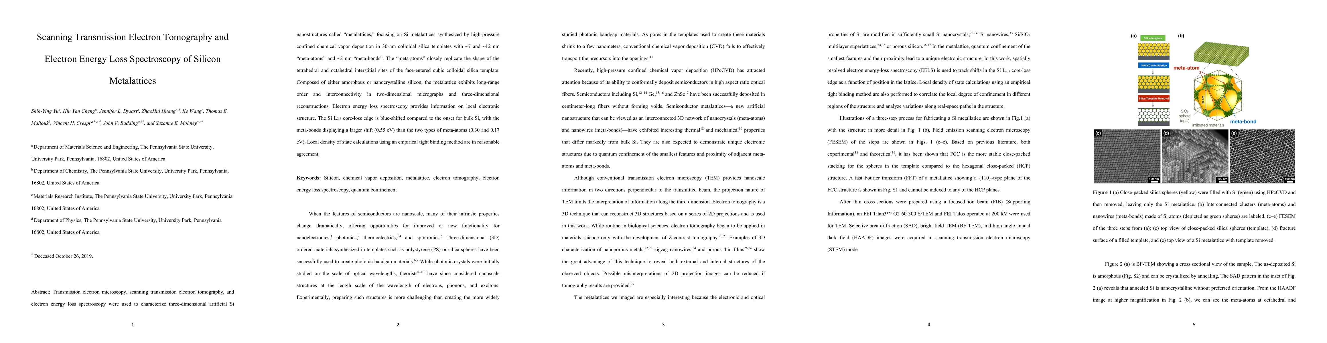
Achieving Minimal Heat Conductivity by Ballistic Confinement in Phononic Metalattices.
|
Weinan Chen, D. Talreja, D. Eichfeld, P. Mahale, N. Nova, H. Y. Cheng, Jennifer L. Russell, Shih-Ying Yu, N. Poilvert, G. Mahan, S. Mohney, V. Crespi, T. Mallouk, J. Badding, B. Foley, V. Gopalan, I. Dabo
|
2020
|
View Paper
|
High Pressure Chemical Vapor Deposition of Hydrogenated Amorphous Silicon Films and Solar Cells
|
R. He, T. Day, J. Sparks, Nichole F. Sullivan, J. Badding
|
2016
|
View Paper
|
Thermoelectric properties of inverse opals
|
G. Mahan, N. Poilvert, V. Crespi
|
2016
|
View Paper
|
Thermal conductivity of silicon nanomeshes: Effects of porosity and roughness
|
S. Wolf, N. Neophytou, H. Kosina
|
2014
|
View Paper
|
Extreme low thermal conductivity in nanoscale 3D Si phononic crystal with spherical pores.
|
Lina Yang, Nuo Yang, Baowen Li
|
2013
|
View Paper
|
Templated Chemically Deposited Semiconductor Optical Fiber Materials
|
J. Sparks, P. Sazio, V. Gopalan, J. Badding
|
2013
|
View Paper
|
Design and Functionality of Colloidal‐Crystal‐Templated Materials—Chemical Applications of Inverse Opals
|
A. Stein, Benjamin E. Wilson, Stephen G. Rudisill
|
2013
|
View Paper
|
Silicon p‐i‐n Junction Fibers
|
R. He, T. Day, M. Krishnamurthi, J. Sparks, P. Sazio, V. Gopalan, J. Badding
|
2013
|
View Paper
|
Nanostructure formation and passivation of large-area black silicon for solar cell applications.
|
Yaoping Liu, T. Lai, Hailing Li, Yan Wang, Z. Mei, Huili Liang, Zhilei Li, Fen Zhang, Wenjing Wang, A. Kuznetsov, Xiaolong Du
|
2012
|
View Paper
|
Direct observation of quantum confinement of Si nanocrystals in Si-rich nitrides
|
P. D. Nguyen, D. Kepaptsoglou, Q. Ramasse, A. Olsen
|
2012
|
View Paper
|
Oxide nanowires for spintronics: materials and devices.
|
Yufeng Tian, S. Bakaul, Tom Wu
|
2012
|
View Paper
|
Zinc Selenide Optical Fibers
|
J. Sparks, R. He, N. Healy, M. Krishnamurthi, A. Peacock, P. Sazio, V. Gopalan, J. Badding
|
2011
|
View Paper
|
Enhancement of the thermoelectric properties in nanoscale and nanostructured materials
|
J. Szczech, J. Higgins, Song Jin
|
2011
|
View Paper
|
Measuring porosity at the nanoscale by quantitative electron tomography.
|
E. Biermans, Leopoldo Molina, K. Batenburg, S. Bals, G. Tendeloo
|
2010
|
View Paper
|
Mid-infrared transmission properties of amorphous germanium optical fibers
|
P. Mehta, M. Krishnamurthi, N. Healy, N. Baril, J. Sparks, P. Sazio, V. Gopalan, J. Badding, A. Peacock
|
2010
|
View Paper
|
Three-dimensional structure of twinned and zigzagged one-dimensional nanostructures using electron tomography
|
H. Kim, Yoon Myung, Y. Cho, D. Jang, C. Jung, Jae-pyoung Ahn, Jeunghee Park
|
2010
|
View Paper
|
3-Dimensional characterization of membrane with nanoporous structure using TEM tomography and image analysis
|
Fenghua She, K. Nihara, Weimin Gao, P. Hodgson, H. Jinnai, L. Kong
|
2010
|
View Paper
|
Silicon Nanowires: A Review on Aspects of their Growth and their Electrical Properties
|
V. Schmidt, J. V. Wittemann, S. Senz, U. Gösele
|
2009
|
View Paper
|
Bulk nanostructured thermoelectric materials: current research and future prospects
|
A. Minnich, M. Dresselhaus, Z. Ren, Gang Chen
|
2009
|
View Paper
|
Electron tomography and holography in materials science.
|
P. Midgley, R. Dunin‐Borkowski
|
2009
|
View Paper
|
Onsite matrix elements of the tight-binding Hamiltonian of a strained crystal: Application to silicon, germanium, and their alloys
|
Y. Niquet, D. Rideau, C. Tavernier, H. Jaouen, X. Blase
|
2009
|
View Paper
|
Computational design of silicon-based direct-band gap nanostructure: Silicon nanonet
|
Dou-xing Li, Jiayou Feng
|
2008
|
View Paper
|
Facile preparation of highly monodisperse small silica spheres (15 to >200 nm) suitable for colloidal templating and formation of ordered arrays.
|
Kurtis D. Hartlen, A. P. T. Athanasopoulos, V. Kitaev
|
2008
|
View Paper
|
Reconstructing a Nanoporous Metal in Three Dimensions: An Electron Tomography Study of Dealloyed Gold Leaf
|
H. Rösner, S. Parida, D. Kramer, C. Volkert, J. Weissmüller
|
2007
|
View Paper
|
High filling fraction gallium phosphide inverse opals by atomic layer deposition
|
E. Graugnard, V. Chawla, D. Lorang, C. Summers
|
2006
|
View Paper
|
Three-dimensional imaging of nonspherical silicon nanoparticles embedded in silicon oxide by plasmon tomography
|
A. Yurtsever, M. Weyland, D. Muller
|
2006
|
View Paper
|
Microstructured Optical Fibers as High-Pressure Microfluidic Reactors
|
P. Sazio, A. Amezcua-Correa, C. Finlayson, J. Hayes, T. Scheidemantel, N. Baril, B. Jackson, D. Won, Feng Zhang, E. R. Margine, V. Gopalan, V. Crespi, J. Badding
|
2006
|
View Paper
|
TiO2 Inverse Opals Fabricated Using Low‐Temperature Atomic Layer Deposition
|
J. King, E. Graugnard, C. Summers
|
2005
|
View Paper
|
Tungsten Nitride Inverse Opals by Atomic Layer Deposition
|
Alessandro Rugge, J. Becker, R. Gordon, S. Tolbert
|
2003
|
View Paper
|
Abrupt topological transitions in the hysteresis curves of ferromagnetic metalattices.
|
Jong E Han, V. Crespi
|
2002
|
View Paper
|
Structure and electronic properties of SiO2/Si multilayer superlattices: Si K edge and L3,2 edge x-ray absorption fine structure study
|
R. Sammynaiken, S. Naftel, T. Sham, K. Cheah, B. Averboukh, R. Huber, Yaochun Shen, G. Qin, Z. C. Ma, W. Zong
|
2002
|
View Paper
|
X-ray absorption fine structure and electron energy loss spectroscopy study of silicon nanowires at the Si L3,2 edge
|
Xuhui Sun, Y. H. Tang, Peng Zhang, S. Naftel, R. Sammynaiken, T. Sham, H. Peng, Yong Zhang, N. B. Wong, Shui-Tong Lee
|
2001
|
View Paper
|
Electron tomography of nanoparticle catalysts on porous supports: A new technique based on Rutherford scattering
|
M. Weyland, P. Midgley, John Meurig Thomas
|
2001
|
View Paper
|
Tuning Fermi-surface properties through quantum confinement in metallic metalattices: new metals from old atoms.
|
Jong E Han, V. Crespi
|
2000
|
View Paper
|
Local chemical states and microstructure of photoluminescent porous silicon studied by means of EELS and TEM
|
Song, Fukuda, Furuya
|
2000
|
View Paper
|
Large-scale synthesis of a silicon photonic crystal with a complete three-dimensional bandgap near 1.5 micrometres
|
A. Blanco, Emmanuel Chomski, S. Grabtchak, M. Ibisate, S. John, S. W. Leonard, C. López, F. Meseguer, H. Míguez, J. Mondia, G. Ozin, O. Toader, H. Driel
|
2000
|
View Paper
|
Single-Crystal Colloidal Multilayers of Controlled Thickness
|
P. Jiang, Jane F. Bertone, K. S. Hwang, V. Colvin
|
1999
|
View Paper
|
Transmission electron energy-loss spectroscopy measurements of the dielectric function of Si/SiO2 multilayers
|
J. Keränen, T. Lepistö, L. Ryen, S. Novikov, E. Olsson
|
1998
|
View Paper
|
Empirical spds^* tight-binding calculation for cubic semiconductors : general method and material parameters
|
J. Jancu, R. Scholz, F. Beltram, F. Bassani
|
1998
|
View Paper
|
Evidence of FCC crystallization of SiO2 nanospheres
|
H. Míguez, F. Meseguer, C. López, A. Mifsud, J. Moya, L. Vázquez
|
1997
|
View Paper
|
Entropy difference between the face-centred cubic and hexagonal close-packed crystal structures
|
L. V. Woodcock
|
1997
|
View Paper
|
ON SURFACE PLASMONS IN POROUS SILICON : MEASUREMENTS OF THE ELECTRON ENERGY LOSS IN ETCHED SILICON NANOCRYSTALS
|
R. M. Sassaki, F. Galembeck, O. Teschke
|
1996
|
View Paper
|
Electron energy loss spectroscopy of single silicon nanocrystals: The conduction band.
|
P. Batson, J. R. Heath
|
1993
|
View Paper
|
Size dependence of plasmon energy in Si clusters
|
M. Mitome, Y. Yamazaki, H. Takagi, T. Nakagiri
|
1992
|
View Paper
|
Quantum size effects on photoluminescence in ultrafine Si particles
|
H. Takagi, H. Ogawa, Y. Yamazaki, A. Ishizaki, T. Nakagiri
|
1990
|
View Paper
|
Three-dimensional morphology of nanoporous gold
|
藤田 武志
|
2008
|
View Paper
|
Z-Contrast tomography: a technique inthree-dimensional nanostructural analysis based on Rutherfordscattering
|
P. Midgley, M. Weyland, John Meurig Thomas, B. Johnson
|
2001
|
View Paper
|
Templates for the Solution of Algebraic Eigenvalue Problems
|
J. Demmel, J. Dongarra, Axel Ruhe, H. A. Vorst, Z. Bai
|
2000
|
View Paper
|
EELS investigation of luminescent ptype silicon
|
|
1996
|
|
Parallel Direct Sparse Solver for Clusters Interface Algorithm from Intel MKL Developer Reference
|
|
2002
|
|
Implicitly Restarted Arnoldi Method, in ed
|
|
2002
|
|
Comments (0)