Publication
Metrics
AI Quick Summary
This paper explores the use of InAs nanowires as STM tips, achieving submicrometer precision in positioning and integrating the tips with GaAs wafers. The STM images exhibit minimal z-noise and lateral stability, confirming effective tunneling through vacuum and minimal tip modification during imaging.
Paper Preview
Abstract
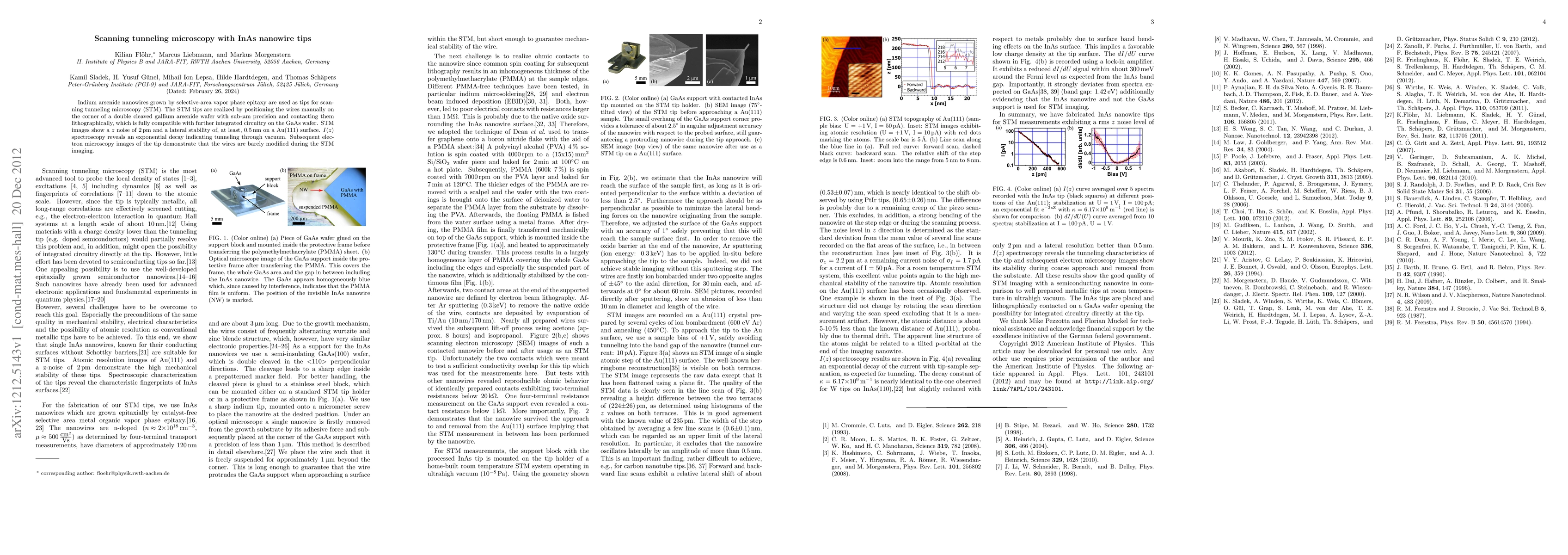
Indium arsenide nanowires grown by selective-area vapor phase epitaxy are used as tips for scanning tunneling microscopy (STM). The STM tips are realized by positioning the wires manually on the corner of a double cleaved gallium arsenide wafer with submicrometer precision and contacting them lithographically, which is fully compatible with further integrated circuitry on the GaAs wafer. STM images show a z-noise of 2 pm and a lateral stability of, at least, 0.5 nm on a Au(111) surface. I(z) spectroscopy reveals an exponential decay indicating tunneling through vacuum. Subsequent electron microscopy images of the tip demonstrate that the wires are barely modified during the STM imaging.
AI Key Findings
Get AI-generated insights about this paper's methodology, results, significance, and more — seven facets brought into focus.
Impact
Paper Details
PDF Preview
Key Terms
Citation Network
Current paper (gray), citations (green), references (blue)
Display is limited for performance on very large graphs.
Discussion 0