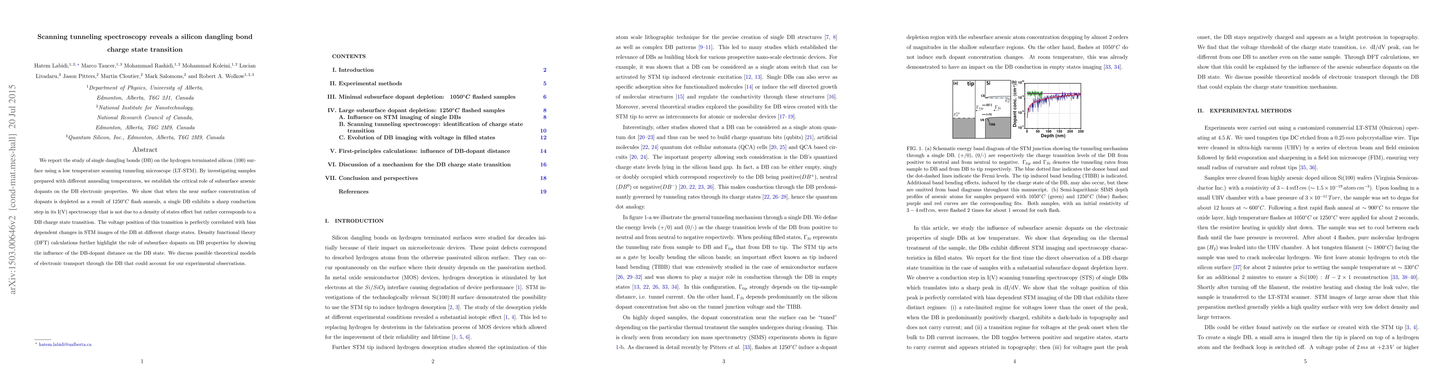
ArxivLens

Quick Summary:

This study uses low-temperature scanning tunneling microscopy to investigate silicon dangling bonds on a hydrogen-terminated silicon (100) surface, revealing a charge state transition in DBs when subsurface arsenic dopants are depleted. The transition is correlated with voltage-dependent changes in STM images and supported by DFT calculations.

Journal Reference: New J. Phys. 17, 073023 (2015)
DOI: 10.1088/1367-2630/17/7/073023
arXiv Id: 1503.00646
Comments: 21 pages, 6 figures
Date Published: 2015-07-22
Date Updated: 2015-07-22

Key Terms (TF-IDF):

db (0.448)
stm (0.278)
electronic (0.185)
charge (0.185)
electronic (0.176)
role (0.162)
charge (0.158)
dft (0.156)
annealing (0.154)
surface (0.153)
transition (0.152)
role (0.151)
conduction (0.150)
functional theory (0.146)
deg (0.143)
prepared (0.143)
bonds (0.142)
density states (0.140)
investigating (0.139)
silicon (0.139)
License: http://arxiv.org/licenses/nonexclusive-distrib/1.0/

Summary:

We report the study of single dangling bonds (DB) on the hydrogen terminated silicon (100) surface using a low temperature scanning tunneling microscope (LT-STM). By investigating samples prepared with different annealing temperatures, we establish the critical role of subsurface arsenic dopants on the DB electronic properties. We show that when the near surface concentration of dopants is depleted as a result of $1250{\deg}C$ flash anneals, a single DB exhibits a sharp conduction step in its I(V) spectroscopy that is not due to a density of states effect but rather corresponds to a DB charge state transition. The voltage position of this transition is perfectly correlated with bias dependent changes in STM images of the DB at different charge states. Density functional theory (DFT) calculations further highlight the role of subsurface dopants on DB properties by showing the influence of the DB-dopant distance on the DB state. We discuss possible theoretical models of electronic transport through the DB that could account for our experimental observations.

Citation & Reference Network Visualization

This graph shows how this paper is connected to other research. The current paper is shown in dark gray, papers that cite it are in green, and papers it references are in blue. You can:

Current Paper
Papers citing this work (Citations)
Papers cited by this work (References)

• Hover over any node to see the paper title

• Click a node to view that paper's details

• Drag nodes to rearrange the graph

• Use the zoom controls (bottom right) to zoom in/out

Citations and References

Title Authors Year Actions
Spatially Resolved Dielectric Loss at the Si/SiO_{2} Interface.
M. Cowie, T. Stock, Procopios Constantinou, Neil J. Curson, P. Grütter
2024
View Paper
Spatially resolved random telegraph fluctuations of a single trap at the Si/SiO2 interface
M. Cowie, Procopios Constantinou, N. Curson, T. Stock, Peter Grutter
2024
View Paper
Atomically Precise Manufacturing of Silicon Electronics
J. Pitters, Jeremiah Croshaw, R. Achal, L. Livadaru, S. Ng, Robert Lupoiu, Taras Chutora, Taleana R Huff, Konrad Walus, R. Wolkow
2024
View Paper
Enhancing the reactivity of Si(100)-Cl toward PBr3 by charging Si dangling bonds.
T. V. Pavlova, V. Shevlyuga
2023
View Paper
A Blueprint for Machine Learning Accelerators Using Silicon Dangling Bonds
S. Ng, H. N. Chiu, Jacob Retallick, K. Waluś
2023
View Paper
Dangling bonds on the Cl- and Br-terminated Si(100) surfaces
T. Pavlova, V. Shevlyuga, B. V. Andryushechkin, K. Eltsov
2022
View Paper
Carbon defect qubit in two-dimensional WS2
Song Li, G. Thiering, P. Udvarhelyi, V. Ivády, Á. Gali
2022
View Paper
Ultra-shallow dopant profiles as in-situ electrodes in scanning probe microscopy
A. Kölker, M. Wolf, M. Koch
2022
View Paper
Necessity of Quantifying Urbach Energy through Scanning Tunneling Spectroscopy.
Soirik Dan, S. Chatterjee, Subham Paramanik, A. Pal
2022
View Paper
Tunable tunnel barriers in a semiconductor via ionization of individual atoms
S. Mueller, Dongjoon Kim, Stephen R McMillan, S. Tjung, J. Repicky, Stephen E. Gant, E. Lang, F. Bergmann, Kevin Werner, E. Chowdhury, A. Asthagiri, M. Flatté, J. Gupta
2021
View Paper
Ionic charge distributions in silicon atomic surface wires.
Jeremiah Croshaw, Taleana R Huff, M. Rashidi, J. Wood, Erika Lloyd, J. Pitters, R. Wolkow
2021
View Paper
Ring charging of a single silicon dangling bond imaged by noncontact atomic force microscopy
N. Turek, S. Godey, D. Deresmes, T. Mélin
2020
View Paper
Ionic Charge Distributions in Silicon Atomic Wires
Jeremiah Croshaw, Taleana R Huff, M. Rashidi, J. Wood, Erika Lloyd, J. Pitters, R. Wolkow
2020
View Paper
Atomic defect classification of the H–Si(100) surface through multi-mode scanning probe microscopy
Jeremiah Croshaw, T. Dienel, Taleana R Huff, R. Wolkow
2020
View Paper
Hydrogen inserted into the Si(100)-2 × 1-H surface: a first-principles study.
T. Pavlova
2020
View Paper
Chlorine insertion and manipulation on the Si(100)- 2×1 -Cl surface in the regime of local supersaturation
T. Pavlova, V. Shevlyuga, B. V. Andryushechkin, K. Eltsov
2020
View Paper
Atomic defects of the hydrogen-terminated Silicon(100)-2x1 surface imaged with STM and nc-AFM
Jeremiah Croshaw, T. Dienel, Taleana R Huff, R. Wolkow
2020
View Paper
Scanned Single-Electron Probe inside a Silicon Electronic Device.
Kevin Ng, B. Voisin, B. Johnson, J. McCallum, J. Salfi, S. Rogge
2020
View Paper
Local removal of silicon layers on Si(1 0 0)-2 × 1 with chlorine-resist STM lithography
T. Pavlova, V. Shevlyuga, B. V. Andryushechkin, G. M. Zhidomirov, K. Eltsov
2020
View Paper
Tunable control over InSb(110) surface conductance utilizing charged defects
S. Mueller, S. Tjung, J. Repicky, E. Lang, Kevin Werner, E. Chowdhury, J. Gupta
2019
View Paper
DFT calculations on the structural and electronic properties of vacancy effects in the silicon nanowires
F. Cruz, H. Alves, F. Sato, A. Carvalho
2019
View Paper
Implementing Functionality in Molecular Self-Assembled Monolayers.
Nemanja Kocić, D. Blank, P. Abufager, N. Lorente, S. Decurtins, Shi‐Xia Liu, J. Repp
2019
View Paper
Moveable Quantum Dot Probe for Detecting Near-Surface Fixed Charges
Taleana R Huff, T. Dienel, M. Rashidi, R. Achal, Wyatt Vine, L. Livadaru, Jeremiah Croshaw, R. Wolkow
2019
View Paper
Electrostatic Landscape of a H-Silicon Surface Probed by a Moveable Quantum Dot.
Taleana R Huff, T. Dienel, M. Rashidi, R. Achal, L. Livadaru, Jeremiah Croshaw, R. Wolkow
2019
View Paper
Binary atomic silicon logic
Taleana R Huff, H. Labidi, Mohammad Mehdi Rashidi, L. Livadaru, T. Dienel, R. Achal, Wyatt Vine, J. Pitters, R. Wolkow
2018
View Paper
SiQAD: A Design and Simulation Tool for Atomic Silicon Quantum Dot Circuits
S. Ng, R. Wolkow, K. Waluś, Jacob Retallick, H. N. Chiu, Robert Lupoiu, L. Livadaru, Taleana R Huff, M. Rashidi, Wyatt Vine, T. Dienel
2018
View Paper
Resistivity change in Joule heat energy dissipation detected by noncontact atomic force microscopy using a silicon tip terminated with/without atomic hydrogen
T. Arai, D. Kura, R. Inamura, M. Tomitori
2018
View Paper
Ab initio characterization of coupling strength for all types of dangling-bond pairs on the hydrogen-terminated Si(100)-2 × 1 surface.
Zahra Shaterzadeh-Yazdi, B. Sanders, G. Dilabio
2018
View Paper
A two-dimensional ON/OFF switching device based on anisotropic interactions of atomic quantum dots on Si(100):H
M. Yengui, E. Duverger, P. Sonnet, D. Riedel
2017
View Paper
Resolving and Tuning Carrier Capture Rates at a Single Silicon Atom Gap State.
M. Rashidi, Erika Lloyd, Taleana R Huff, R. Achal, M. Taucer, Jeremiah Croshaw, R. Wolkow
2017
View Paper
Tip-induced passivation of dangling bonds on hydrogenated Si(100)-2 × 1
N. Pavliček, Z. Majzik, G. Meyer, L. Gross
2017
View Paper
Toward Atom Scale Ultra Low Power Classical Circuitry and Quantum Circuitry
R. Wolkow
2017
View Paper
Binary atomic silicon logic
Taleana R Huff, H. Labidi, M. Rashidi, L. Livadaru, T. Dienel, R. Achal, Wyatt Vine, J. Pitters, R. Wolkow
2017
View Paper
Atomic White-Out: Enabling Atomic Circuitry through Mechanically Induced Bonding of Single Hydrogen Atoms to a Silicon Surface.
Taleana R Huff, H. Labidi, M. Rashidi, M. Koleini, R. Achal, M. Salomons, R. Wolkow
2017
View Paper
Imagerie, manipulation et contact électronique atome par atome sur la surface Si(100):H avec le microscope à effet tunnel basse température à 4 pointes
Delphine Sordes
2017
View Paper
Optimizing surface defects for atomic-scale electronics: Si dangling bonds
P. Scherpelz, G. Galli
2017
View Paper
Indications of chemical bond contrast in AFM images of a hydrogen-terminated silicon surface
H. Labidi, M. Koleini, Taleana R Huff, M. Salomons, Martin Cloutier, J. Pitters, R. Wolkow
2017
View Paper
Correlation Effects in Scanning Tunneling Microscopy Images of Molecules Revealed by Quantum Monte Carlo.
Matteo Barborini, S. Sorella, M. Rontani, S. Corni
2016
View Paper
Search for a metallic dangling-bond wire on n-doped H-passivated semiconductor surfaces
M. Engelund, Nick R. Papior, Pedro Brandimarte, Thomas Frederiksen, A. Garcia-Lekue, Daniel Sánchez-Portal
2016
View Paper
Time-Resolved Imaging of Negative Differential Resistance on the Atomic Scale.
M. Rashidi, M. Taucer, I. Ozfidan, Erika Lloyd, M. Koleini, H. Labidi, J. Pitters, J. Maciejko, R. Wolkow
2016
View Paper
Single-Molecule Rotational Switch on a Dangling Bond Dimer Bearing.
S. Godlewski, H. Kawai, M. Kolmer, Rafal Zuzak, A. Echavarren, C. Joachim, M. Szymoński, M. Saeys
2016
View Paper
The butterfly - a well-defined constant-current topography pattern on Si(001):H and Ge(001):H resulting from current-induced defect fluctuations.
M. Engelund, S. Godlewski, M. Kolmer, Rafal Zuzak, B. Such, T. Frederiksen, M. Szymoński, D. Sánchez-Portal
2016
View Paper
Communication: Visualization and spectroscopy of defects induced by dehydrogenation in individual silicon nanocrystals.
D. A. Kislitsyn, Jon M. Mills, V. Kocevski, Sheng-Kuei Chiu, W. DeBenedetti, C. Gervasi, B. Taber, Ariel E Rosenfield, O. Eriksson, J. Rusz, A. Goforth, G. Nazin
2016
View Paper
Diels-Alder attachment of a planar organic molecule to a dangling bond dimer on a hydrogenated semiconductor surface.
S. Godlewski, H. Kawai, M. Engelund, M. Kolmer, Rafal Zuzak, A. Garcia-Lekue, G. Novell-Leruth, A. Echavarren, D. Sánchez-Portal, C. Joachim, M. Saeys
2016
View Paper
The surface electronic structure of silicon terminated (100) diamond
A. Schenk, A. Tadich, Anton Tadich, M. Sear, Dongchen Qi, Andrew T. S. Wee, Alastair Stacey, C. Pakes
2016
View Paper
Electrical current through individual pairs of phosphorus donor atoms and silicon dangling bonds
K. Ambal, P. Rahe, A. Payne, J. Slinkman, C. C. Williams, C. Boehme
2016
View Paper
Time-resolved single dopant charge dynamics in silicon
M. Rashidi, J. Burgess, M. Taucer, R. Achal, J. Pitters, S. Loth, R. Wolkow
2015
View Paper
Two-Dimensional Pnictogen Honeycomb Lattice: Structure, On-Site Spin-Orbit Coupling and Spin Polarization
Jason Lee, Wen-Chuan Tian, Weiliang Wang, D. Yao
2014
View Paper
Surface Hydrogenation of the Si(100)-2×1 and Electronic Properties of Silicon Dangling Bonds on the Si(100):H Surfaces
D. Riedel
2017
View Paper
Mechanisms of Local and Nonlocal Atomic Manipulation with a Scanning Tunnelling MIcroscope
K. Rusimova
2016
View Paper
Time Resolved Single Dopant Charge Dynamics in Silicon
M. Rashidi, J. Burgess, M. Taucer, R. Achal, J. Pitters, S. Loth, R. Wolkow, J A Mol, J. Salfi, J. A. Miwa, M. Y. Simmons, S. Rogge, B Voisin, J. Bocquel, R. Rahman, D. Kitchen, A. Richardella, J. M. Tang, M. Flatté, A. Yazdani, C Grosse, M. Etzkorn, K. Kuhnke, K. Kern, S Loth, S. Baumann, C. Lutz, D. Eigler, A. Heinrich, C Saunus, J. R. Bindel, M. Pratzer, M. Morgenstern, S Yan, D.-J Choi, J. Burgess, S. Rolf-Pissarczyk, M Rezeq, J. Pitters, R. Wolkow, J J Boland
View Paper
An ultra-fast method for scanning tunneling spectroscopy
Hamed Alemansour, S. O. R. Moheimani, James H G Owen, J. N. Randall, E. Fuchs
View Paper

Comments (0)

This website uses cookies to ensure you get the best experience. Learn more