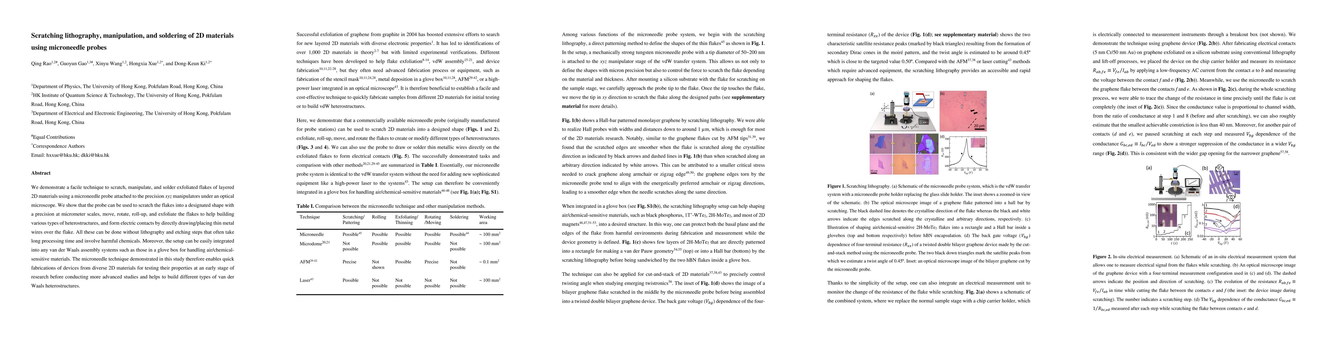
Publication
Metrics
AI Quick Summary
This paper presents a microneedle probe technique for precise scratching, manipulation, and soldering of 2D materials without lithography, enabling quick device fabrication and heterostructure assembly for early-stage research. The method avoids lengthy and harmful chemical processes, facilitating the integration into glove box systems.
Paper Preview
Abstract
We demonstrate a facile technique to scratch, manipulate, and solder exfoliated flakes of layered 2D materials using a microneedle probe attached to the precision xyz manipulators under an optical microscope. We show that the probe can be used to scratch the flakes into a designated shape with a precision at micrometer scales, move, rotate, roll-up, and exfoliate the flakes to help building various types of heterostructures, and form electric contacts by directly drawing/placing thin metal wires over the flake. All these can be done without lithography and etching steps that often take long processing time and involve harmful chemicals. Moreover, the setup can be easily integrated into any van der Waals assembly systems such as those in a glove box for handling air/chemical-sensitive materials. The microneedle technique demonstrated in this study therefore enables quick fabrications of devices from diverse 2D materials for testing their properties at an early stage of research before conducting more advanced studies and helps to build different types of van der Waals heterostructures.
AI Key Findings
Get AI-generated insights about this paper's methodology, results, significance, and more — seven facets brought into focus.
Impact
Paper Details
Authors
PDF Preview
Key Terms
Citation Network
Current paper (gray), citations (green), references (blue)
Display is limited for performance on very large graphs.
Discussion 0