Publication
Metrics
AI Quick Summary
This paper introduces a high-throughput electrochemiluminescence (ECL) method for detecting sub-micron defects in thin insulating films, achieving features as small as 2.5 nm lines and 35 nm pinholes. The method leverages optimized ECL conditions to enhance detection sensitivity and throughput, demonstrating its potential for automated discovery in multifunctional films.
Paper Preview
Abstract
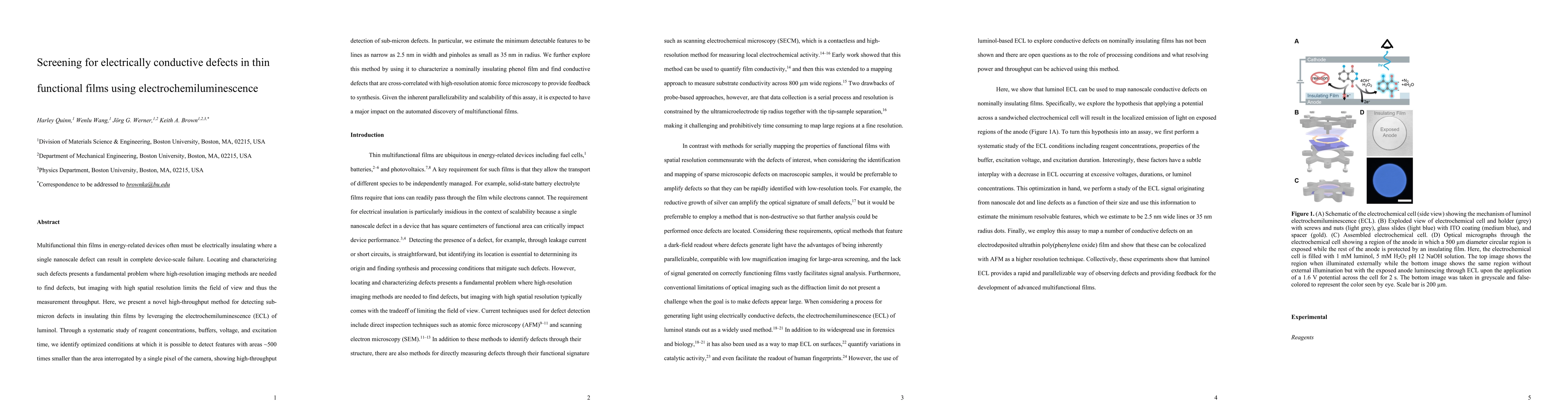
Multifunctional thin films in energy-related devices often must be electrically insulating where a single nanoscale defect can result in complete device-scale failure. Locating and characterizing such defects presents a fundamental problem where high-resolution imaging methods are needed to find defects, but imaging with high spatial resolution limits the field of view and thus the measurement throughput. Here, we present a novel high-throughput method for detecting sub-micron defects in insulating thin films by leveraging the electrochemiluminescence (ECL) of luminol. Through a systematic study of reagent concentrations, buffers, voltage, and excitation time, we identify optimized conditions at which it is possible to detect features with areas ~500 times smaller than the area interrogated by a single pixel of the camera, showing high-throughput detection of sub-micron defects. In particular, we estimate the minimum detectable features to be lines as narrow as 2.5 nm in width and pinholes as small as 35 nm in radius. We further explore this method by using it to characterize a nominally insulating phenol film and find conductive defects that are cross-correlated with high-resolution atomic force microscopy to provide feedback to synthesis. Given the inherent parallelizability and scalability of this assay, it is expected to have a major impact on the automated discovery of multifunctional films.
AI Key Findings
Get AI-generated insights about this paper's methodology, results, significance, and more — seven facets brought into focus.
Impact
Paper Details
Authors
PDF Preview
Key Terms
Citation Network
Current paper (gray), citations (green), references (blue)
Display is limited for performance on very large graphs.
Discussion 0