Publication
Metrics
AI Quick Summary
Researchers explored alternative plasmonic materials to overcome losses in existing metals for novel devices, proposing a comparative study of various materials with improved performance characteristics.
Paper Preview
Abstract
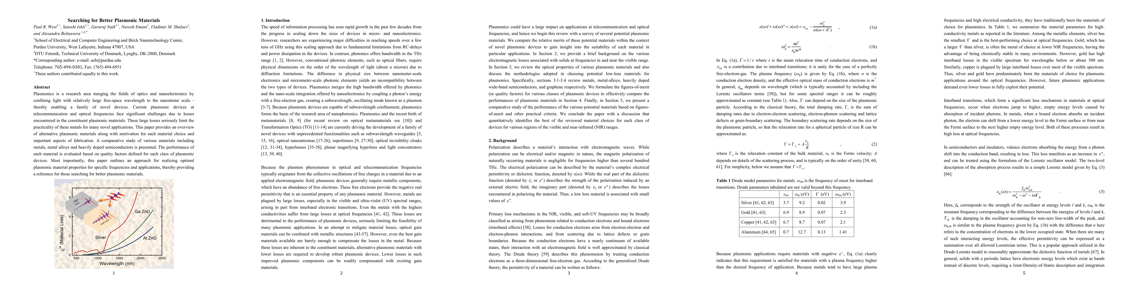
Plasmonics is a research area merging the fields of optics and nanoelectronics by confining light with relatively large free-space wavelength to the nanometer scale - thereby enabling a family of novel devices. Current plasmonic devices at telecommunication and optical frequencies face significant challenges due to losses encountered in the constituent plasmonic materials. These large losses seriously limit the practicality of these metals for many novel applications. This paper provides an overview of alternative plasmonic materials along with motivation for each material choice and important aspects of fabrication. A comparative study of various materials including metals, metal alloys and heavily doped semiconductors is presented. The performance of each material is evaluated based on quality factors defined for each class of plasmonic devices. Most importantly, this paper outlines an approach for realizing optimal plasmonic material properties for specific frequencies and applications, thereby providing a reference for those searching for better plasmonic materials.
AI Key Findings
Get AI-generated insights about this paper's methodology, results, significance, and more — seven facets brought into focus.
Impact
Paper Details
PDF Preview
Key Terms
Citation Network
Current paper (gray), citations (green), references (blue)
Display is limited for performance on very large graphs.
Discussion 0