Selective area epitaxy of in-plane HgTe nanostrcutures on CdTe(001) substrate
Publication
Metrics
AI Quick Summary
This paper details the selective growth of in-plane HgTe nanostructures on CdTe(001) using molecular beam epitaxy, enabling diverse nanostructure forms and minimal parasitic growth even at low temperatures. The technique shows good electrical homogeneity and epitaxial relationship, paving the way for advanced electronic applications.
Paper Preview
Abstract
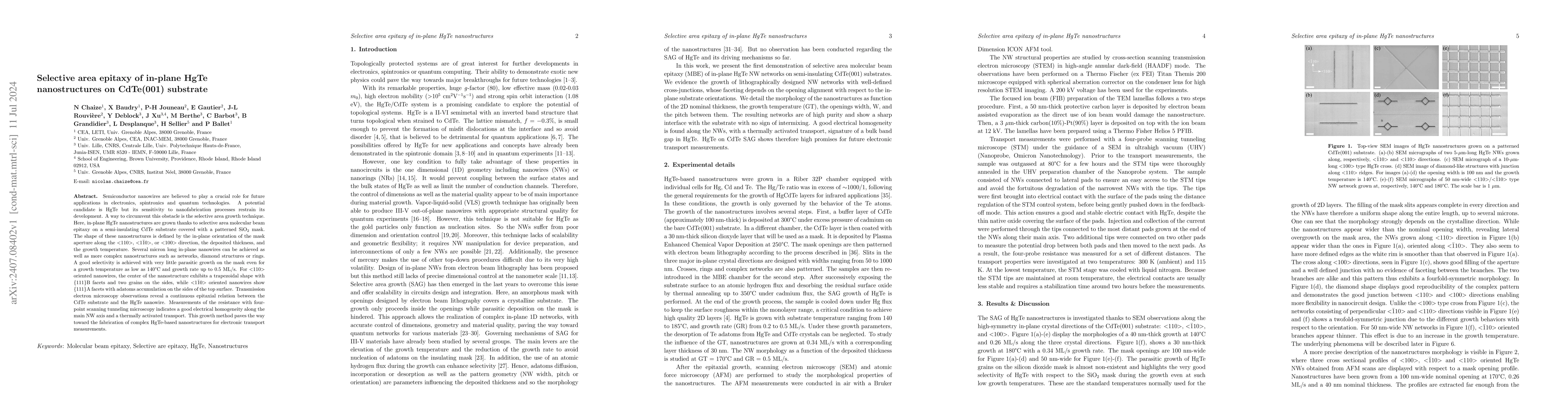
Semiconductor nanowires are believed to play a crucial role for future applications in electronics, spintronics and quantum technologies. A potential candidate is HgTe but its sensitivity to nanofabrication processes restrain its development. A way to circumvent this obstacle is the selective area growth technique. Here, in-plane HgTe nanostructures are grown thanks to selective area molecular beam epitaxy on a semi-insulating CdTe substrate covered with a patterned SiO$_{\mathrm{2}}$ mask. The shape of these nanostructures is defined by the in-plane orientation of the mask aperture along the <$110$>, <$1\bar{\mathrm{1}}0$>, or <$100$> direction, the deposited thickness, and the growth temperature. Several micron long in-plane nanowires can be achieved as well as more complex nanostructures such as networks, diamond structures or rings. A good selectivity is achieved with very little parasitic growth on the mask even for a growth temperature as low as $140${\deg}C and growth rate up to $0.5$ ML/s. For <$110$> oriented nanowires, the center of the nanostructure exhibits a trapezoidal shape with {$111$}B facets and two grains on the sides, while <$1\bar{\mathrm{1}}0$> oriented nanowires show {$111$}A facets with adatoms accumulation on the sides of the top surface. Transmission electron microscopy observations reveal a continuous epitaxial relation between the CdTe substrate and the HgTe nanowire. Measurements of the resistance with fourpoint scanning tunneling microscopy indicates a good electrical homogeneity along the main NW axis and a thermally activated transport. This growth method paves the way toward the fabrication of complex HgTe-based nanostructures for electronic transport measurements.
AI Key Findings
Get AI-generated insights about this paper's methodology, results, significance, and more — seven facets brought into focus.
Impact
Paper Details
Authors
PDF Preview
Citation Network
Current paper (gray), citations (green), references (blue)
Display is limited for performance on very large graphs.
Discussion 0