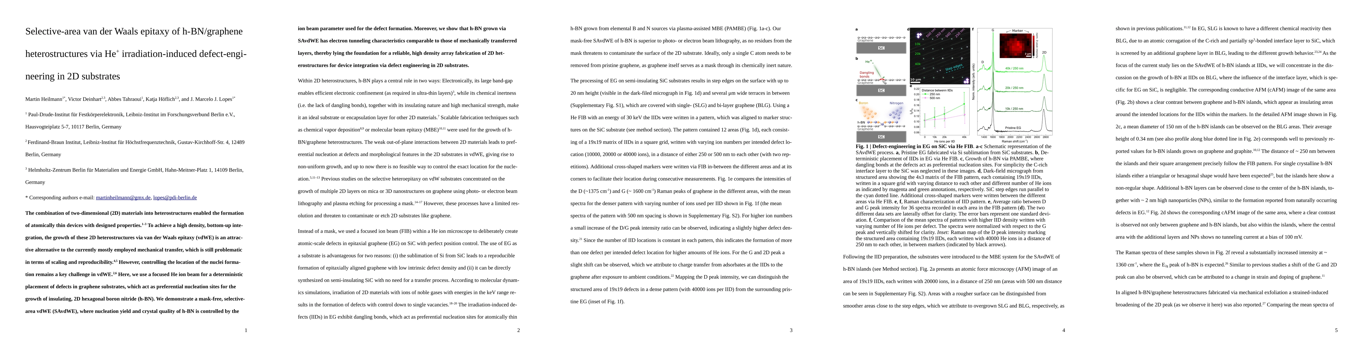
Summary
The combination of two-dimensional (2D) materials into heterostructures enabled the formation of atomically thin devices with designed properties. To achieve a high density, bottom-up integration, the growth of these 2D heterostructures via van der Waals epitaxy (vdWE) is an attractive alternative to the currently mostly employed mechanical transfer, which is still problematic in terms of scaling and reproducibility. However, controlling the location of the nuclei formation remains a key challenge in vdWE. Here, we use a focused He ion beam for a deterministic placement of defects in graphene substrates, which act as preferential nucleation sites for the growth of insulating, 2D hexagonal boron nitride (h-BN). We demonstrate a mask-free, selective-area vdWE (SAvdWE), where nucleation yield and crystal quality of h-BN is controlled by the ion beam parameter used for the defect formation. Moreover, we show that h-BN grown via SAvdWE has electron tunneling characteristics comparable to those of mechanically transferred layers, thereby lying the foundation for a reliable, high density array fabrication of 2D heterostructures for device integration via defect engineering in 2D substrates.
AI Key Findings
Get AI-generated insights about this paper's methodology, results, and significance.
Paper Details
PDF Preview
Key Terms
Citation Network
Current paper (gray), citations (green), references (blue)
Display is limited for performance on very large graphs.
Similar Papers
Found 4 papersHybridization in van der Waals epitaxy of PtSe2/h-BN and PtSe2/graphene heterostructures
Iann C. Gerber, Abdelkarim Ouerghi, Jose Avila et al.
Versatile van der Waals Heterostructures of Gamma-GeSe with h-BN/Graphene/MoS2
Pu Wang, Yongqing Cai, Binghan He et al.
| Title | Authors | Year | Actions |
|---|
Comments (0)