Publication
Metrics
AI Quick Summary
This paper presents a method to selectively form luminescent defect-centers in hexagonal boron nitride (hBN) for single photon emitters (SPEs) via boron diffusion manipulation during atmospheric pressure chemical vapor deposition. The technique, termed gettering, allows precise control over the emission properties of hBN SPEs, paving the way for integration into photonic architectures.
Paper Preview
Abstract
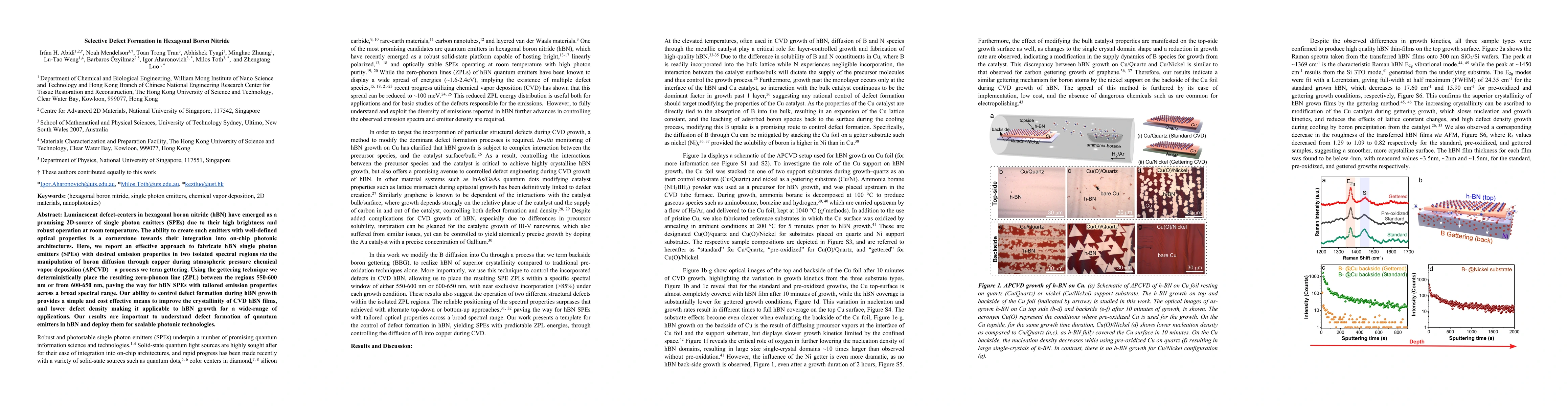
Luminescent defect-centers in hexagonal boron nitride (hBN) have emerged as a promising 2D-source of single photon emitters (SPEs) due to their high brightness and robust operation at room temperature. The ability to create such emitters with well-defined optical properties is a cornerstone towards their integration into on-chip photonic architectures. Here, we report an effective approach to fabricate hBN single photon emitters (SPEs) with desired emission properties in two isolated spectral regions via the manipulation of boron diffusion through copper during atmospheric pressure chemical vapor deposition (APCVD)--a process we term gettering. Using the gettering technique we deterministically place the resulting zero-phonon line (ZPL) between the regions 550-600 nm or from 600-650 nm, paving the way for hBN SPEs with tailored emission properties across a broad spectral range. Our ability to control defect formation during hBN growth provides a simple and cost-effective means to improve the crystallinity of CVD hBN films, and lower defect density making it applicable to hBN growth for a wide range of applications. Our results are important to understand defect formation of quantum emitters in hBN and deploy them for scalable photonic technologies.
AI Key Findings
Get AI-generated insights about this paper's methodology, results, significance, and more — seven facets brought into focus.
Impact
Paper Details
PDF Preview
Key Terms
Citation Network
Current paper (gray), citations (green), references (blue)
Display is limited for performance on very large graphs.
Discussion 0