Publication
Metrics
Quick Actions
Quick Answers
What methodology did the authors use?
Self‑aligned heterogeneous integration of single‑crystal diamond nanobeams hosting SiV centers into TiO2 photonic circuits via conformal atomic‑layer deposition, combined with inverse‑design photonic structures for efficient coupling and broadband extraction. More in Methodology →
What are the key results?
Achieved a minimum Purcell factor of 6 (potentially 150 with higher‑Q cavities) by resonantly coupling SiV centers to a TiO2 photonic‑crystal cavity. — Demonstrated optical spin initialization and readout through the TiO2 circuit with 72% fidelity and a spin‑relaxation time of 130 ns. More in Key Results →
Why is this work significant?
Provides a scalable, low‑loss route to integrate high‑quality solid‑state quantum emitters with mature thin‑film photonic platforms, enabling quantum repeaters, networks, and on‑chip quantum photonic devices. More in Significance →
What are the main limitations?
Cavity quality factors limited by fabrication deviations (corner rounding, width variations) rather than the integration process. — Purcell enhancement experiment limited by low Q (920) and detuning, partly due to ALD‑induced thickness mismatch. More in Limitations →
Abstract
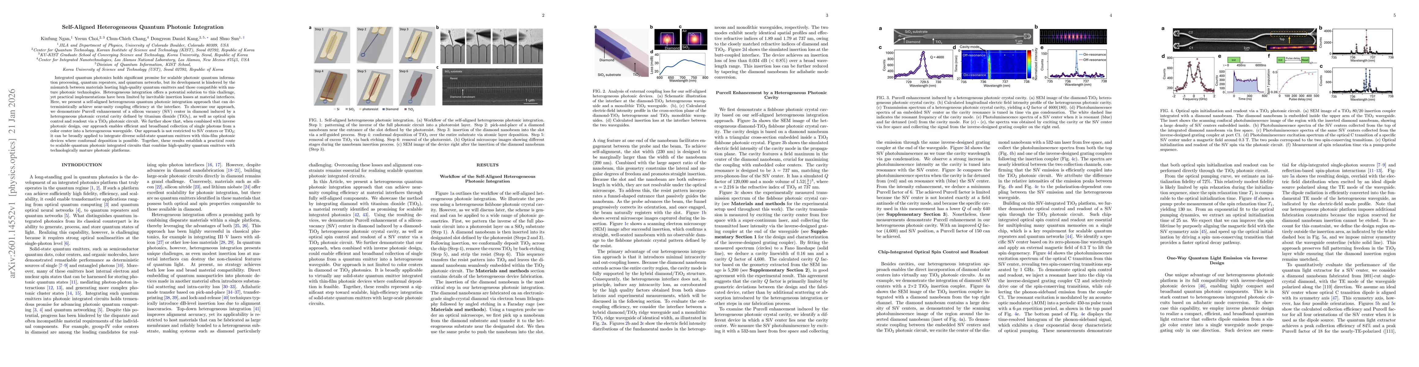
Integrated quantum photonics holds significant promise for scalable photonic quantum information processing, quantum repeaters, and quantum networks, but its development is hindered by the mismatch between materials hosting high-quality quantum emitters and those compatible with mature photonic technologies. Heterogeneous integration offers a potential solution to this challenge, yet practical implementations have been limited by inevitable insertion losses at material interfaces. Here, we present a self-aligned heterogeneous quantum photonic integration approach that can deterministically achieve near-unity coupling efficiency at the interface. To showcase our approach, we demonstrate Purcell enhancement of a silicon vacancy (SiV) center in diamond induced by a heterogeneous photonic crystal cavity defined by titanium dioxide (TiO2), as well as optical spin control and readout via a TiO2 photonic circuit. We further show that, when combined with inverse photonic design, our approach enables efficient and broadband collection of single photons from a color center into a heterogeneous waveguide. Our approach is not restricted to SiV centers or TiO2; it can be broadly applied to integrate diverse solid-state quantum emitters with thin-film photonic devices where conformal deposition is possible. Together, these results establish a practical route to scalable quantum photonic integrated circuits that combine high-quality quantum emitters with technologically mature photonic platforms.
AI Key Findings
Generated Jan 22, 2026
Methodology — What approach did the authors take?
Self‑aligned heterogeneous integration of single‑crystal diamond nanobeams hosting SiV centers into TiO2 photonic circuits via conformal atomic‑layer deposition, combined with inverse‑design photonic structures for efficient coupling and broadband extraction.
Key Results — What are the main findings?
- Achieved a minimum Purcell factor of 6 (potentially 150 with higher‑Q cavities) by resonantly coupling SiV centers to a TiO2 photonic‑crystal cavity.
- Demonstrated optical spin initialization and readout through the TiO2 circuit with 72% fidelity and a spin‑relaxation time of 130 ns.
- Realized an inverse‑designed one‑way quantum light extractor with 84% collection efficiency and a Purcell factor of 18 over a 5.5‑nm bandwidth.
Significance — Why does this research matter?
Provides a scalable, low‑loss route to integrate high‑quality solid‑state quantum emitters with mature thin‑film photonic platforms, enabling quantum repeaters, networks, and on‑chip quantum photonic devices.
Technical Contribution — What is the technical contribution?
A self‑aligned, near‑unity coupling scheme that embeds diamond nanobeams into TiO2 waveguides using conformal ALD, eliminating interface loss and enabling efficient spin control and broadband photon extraction.
Novelty — What is new about this work?
First demonstration of deterministic near‑unity emitter‑waveguide coupling, spin control via integrated TiO2 circuits, and broadband one‑way photon extraction using inverse design, applicable to diverse solid‑state emitters.
Limitations — What are the limitations of this study?
- Cavity quality factors limited by fabrication deviations (corner rounding, width variations) rather than the integration process.
- Purcell enhancement experiment limited by low Q (920) and detuning, partly due to ALD‑induced thickness mismatch.
Future Work — What did the authors propose for future work?
- Improve cavity Q to >10 k and Purcell factors >300 through refined lithography and design tolerance.
- Develop faster conformal deposition (PVD/PECVD) and deterministic emitter placement for large‑scale, multi‑emitter circuits.
Paper Details
How to Cite This Paper
@article{chang2026self,
title = {Self-Aligned Heterogeneous Quantum Photonic Integration},
author = {Chang, Chun-Chieh and Kang, Dongyeon Daniel and Ngan, Kinfung and others},
year = {2026},
eprint = {2601.14552},
archivePrefix = {arXiv},
primaryClass = {physics.optics},
}
Chang, C., Kang, D., Ngan, K., Sun, S., & Choi, Y. (2026). Self-Aligned Heterogeneous Quantum Photonic Integration. arXiv. https://arxiv.org/abs/2601.14552
Chang, Chun-Chieh, et al. "Self-Aligned Heterogeneous Quantum Photonic Integration." arXiv, 2026, arxiv.org/abs/2601.14552.
PDF Preview
Similar Papers
Found 4 papersSelf-aligned photonic defect microcavities with site-controlled quantum dots
C. -W. Shih, I. Limame, C. C. Palekar et al.
Multi-material heterogeneous integration on a 3-D Photonic-CMOS platform
Luigi Ranno, Jia Xu Brian Sia, Khoi Phuong Dao et al.
Comments (0)