The research introduces a self-aligned local electrolyte gating technique for 2D materials with nanoscale resolution, utilizing a solid-polymer electrolyte gate and an ion-impenetrable e-beam-defined resist mask to create excess charges on the surface of 2D conductors.
Publication
Metrics
AI Quick Summary
This paper presents a self-aligned electrolyte gating technique for 2D materials that achieves nanoscale resolution, overcoming limitations of traditional capacitive gating. The method uses a solid-polymer electrolyte and a mask to create sharp, tunable p-n junctions in graphene, demonstrating potential for optoelectronic applications and novel devices like thermopile photodetectors.
Quick Answers
What methodology did the authors use?
The research introduces a self-aligned local electrolyte gating technique for 2D materials with nanoscale resolution, utilizing a solid-polymer electrolyte gate and an ion-impenetrable e-beam-defined resist mask to create excess charges on the surface of 2D conductors. More in Methodology →
What are the key results?
The technique achieves high carrier density variations of Δn = 10^14 cm^-2 across a length of 10 nm at the mask boundaries. — A strong in-plane electric field of 6 × 10^8 V m^-1 is generated across the junction. More in Key Results →
Why is this work significant?
This dielectric-free gating concept overcomes limitations of traditional capacitive coupling methods, enabling stronger and more uniform electric fields at nanometer scales, which is crucial for smaller, faster, and more efficient 2D material-based devices. More in Significance →
What are the main limitations?
The paper does not discuss scalability for mass production. — Potential long-term stability of the electrolyte and mask materials is not addressed. More in Limitations →
Abstract
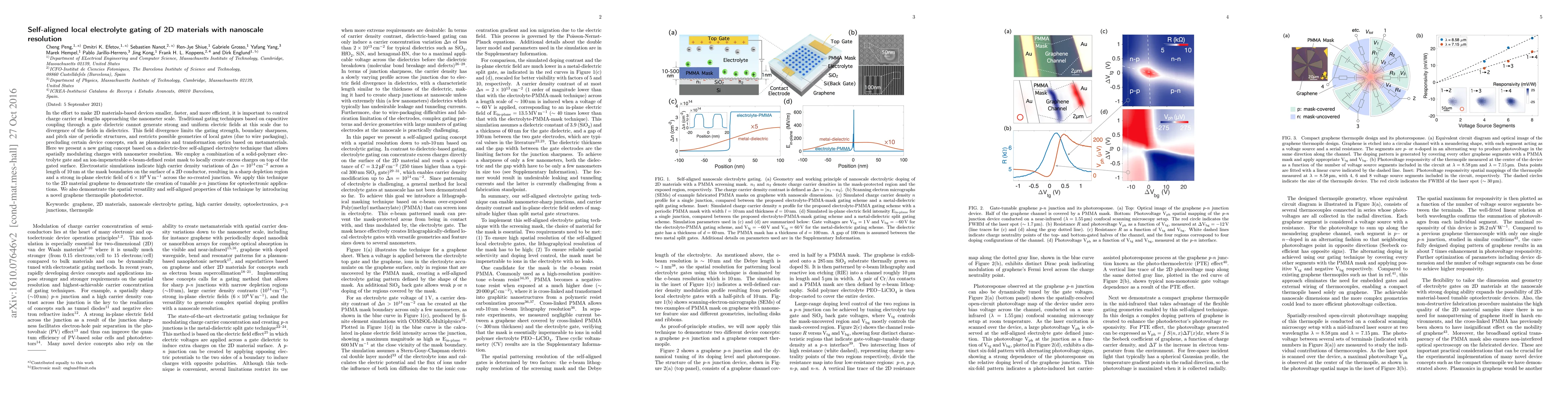
In the effort to make 2D materials-based devices smaller, faster, and more efficient, it is important to control charge carrier at lengths approaching the nanometer scale. Traditional gating techniques based on capacitive coupling through a gate dielectric cannot generate strong and uniform electric fields at this scale due to divergence of the fields in dielectrics. This field divergence limits the gating strength, boundary sharpness, and pitch size of periodic structures, and restricts possible geometries of local gates (due to wire packaging), precluding certain device concepts, such as plasmonics and transformation optics based on metamaterials. Here we present a new gating concept based on a dielectric-free self-aligned electrolyte technique that allows spatially modulating charges with nanometer resolution. We employ a combination of a solid-polymer electrolyte gate and an ion-impenetrable e-beam-defined resist mask to locally create excess charges on top of the gated surface. Electrostatic simulations indicate high carrier density variations of $\Delta n =10^{14}\text{cm}^{-2}$ across a length of 10 nm at the mask boundaries on the surface of a 2D conductor, resulting in a sharp depletion region and a strong in-plane electric field of $6\times10^8 \text{Vm}^{-1}$ across the so-created junction. We apply this technique to the 2D material graphene to demonstrate the creation of tunable p-n junctions for optoelectronic applications. We also demonstrate the spatial versatility and self-aligned properties of this technique by introducing a novel graphene thermopile photodetector.
Key Findings, in focus
Seven facets of this paper, analysed and brought into focus by AI.
This dielectric-free gating concept overcomes limitations of traditional capacitive coupling methods, enabling stronger and more uniform electric fields at nanometer scales, which is crucial for smaller, faster, and more efficient 2D material-based devices.
- The technique achieves high carrier density variations of Δn = 10^14 cm^-2 across a length of 10 nm at the mask boundaries.
- A strong in-plane electric field of 6 × 10^8 V m^-1 is generated across the junction.
- Tunable p-n junctions in graphene are demonstrated for optoelectronic applications.
- A novel graphene thermopile photodetector is introduced, showcasing the spatial versatility and self-aligned properties of the technique.
This dielectric-free gating concept overcomes limitations of traditional capacitive coupling methods, enabling stronger and more uniform electric fields at nanometer scales, which is crucial for smaller, faster, and more efficient 2D material-based devices.
The paper presents a novel method for local electrolyte gating of 2D materials, offering high carrier density modulation and strong electric fields with nanoscale resolution.
The self-aligned electrolyte gating technique overcomes limitations of conventional dielectric-based gating methods, providing enhanced control over charge carrier distribution in 2D materials for advanced optoelectronic devices.
- The paper does not discuss scalability for mass production.
- Potential long-term stability of the electrolyte and mask materials is not addressed.
- Exploration of different 2D materials beyond graphene for broader applicability.
- Investigating the technique's performance under varying environmental conditions.
Impact
Paper Details
PDF Preview
Key Terms
Citation Network
Current paper (gray), citations (green), references (blue)
Display is limited for performance on very large graphs.
Discussion 0