The study combines crystal-facet engineering on curved Cu surfaces with complementary microscopy (STM/LEED) and spectroscopy (XPS) techniques, supported by theoretical calculations to determine structural and electronic properties of two distinct 2D phosphorus phases grown in a single-step process.
Self-Aligned Metallic-Semiconducting Phosphorus Nanoarrays Driven by Facet Engineering
Publication
Metrics
Quick Answers
What methodology did the authors use?
The study combines crystal-facet engineering on curved Cu surfaces with complementary microscopy (STM/LEED) and spectroscopy (XPS) techniques, supported by theoretical calculations to determine structural and electronic properties of two distinct 2D phosphorus phases grown in a single-step process. More in Methodology →
What are the key results?
Two distinct 2D phosphorus phases are stabilized: hexagonal blue phosphorene on Cu(111) terraces and a previously unreported skewed-square phosphorus phase on Cu(513) facets. — The skewed-square phase exhibits semiconducting character, in contrast to the metallic behavior of blue phosphorene, enabling a metal-to-semiconducting transition of the 2D phosphorus layer over the substrate. More in Key Results →
Why is this work significant?
Demonstrates crystal-facet engineering as a practical route to discover and stabilize emergent 2D material phases on high-index substrates, and to engineer nanoscale electronic structures with a simple, scalable growth process. More in Significance →
What are the main limitations?
The study focuses on phosphorus on curved Cu surfaces; generalization to other material systems requires further validation. — Observations are largely surface- and interface- sensitive; long-term stability and device integration remain to be explored. More in Limitations →
Abstract
Two-dimensional (2D) materials often require specific substrate terminations for epitaxial stabilization, yet the search for suitable templates has largely focused on low-index metal surfaces, which may not provide the optimal conditions for the growth of new phases. Here, we show that crystal-facet engineering on curved Cu surfaces enables the stabilization, within a single preparation step, of two distinct 2D phosphorus phases with different electronic properties. Hexagonal blue phosphorene forms on Cu(111) terraces, whereas a previously unreported skewed-square phosphorus phase is stabilized on Cu(513) facets. By combining complementary microscopy and spectroscopy techniques with theoretical calculations, we determine the structural and electronic properties of this new phase, which displays semiconducting character, in contrast to the metallic behavior of blue phosphorene. The coexistence of these two competing phases gives rise to a metal-to-semiconducting transition of the 2D phosphorus layer over the substrate. Locally, the competition between the two phases gives rise to self-aligned nanoarrays of alternating metallic and semiconducting phosphorus terraces. These results establish crystal-facet engineering as a practical route for discovering and stabilizing emergent 2D material phases on high-index substrates, while also enabling the engineering of nanostructures with tailored electronic properties through a simple and scalable growth process.
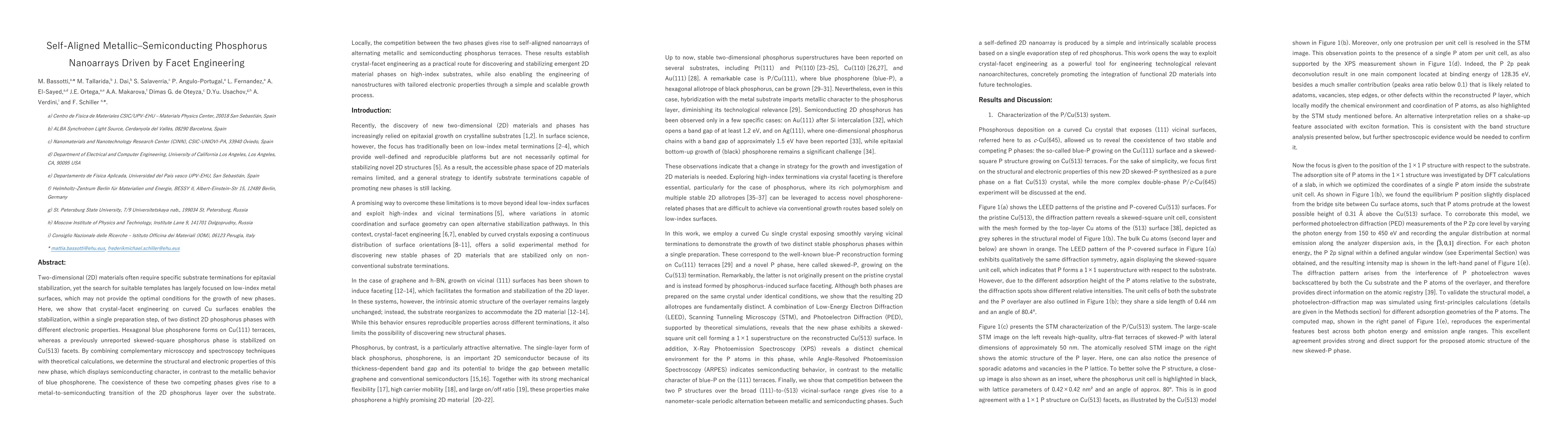
Key Findings, in focus
Seven facets of this paper, analysed and brought into focus by AI.
Demonstrates crystal-facet engineering as a practical route to discover and stabilize emergent 2D material phases on high-index substrates, and to engineer nanoscale electronic structures with a simple, scalable growth process.
- Two distinct 2D phosphorus phases are stabilized: hexagonal blue phosphorene on Cu(111) terraces and a previously unreported skewed-square phosphorus phase on Cu(513) facets.
- The skewed-square phase exhibits semiconducting character, in contrast to the metallic behavior of blue phosphorene, enabling a metal-to-semiconducting transition of the 2D phosphorus layer over the substrate.
- Local phase competition leads to self-aligned nanoarrays of alternating metallic and semiconducting phosphorus terraces.
Demonstrates crystal-facet engineering as a practical route to discover and stabilize emergent 2D material phases on high-index substrates, and to engineer nanoscale electronic structures with a simple, scalable growth process.
Introduction of a single-step growth route that uses curved Cu substrates exposing a spectrum of facet orientations to stabilize two distinct phosphorus phases with contrasting electronic properties, and direct observation of self-aligned metallic and semiconducting P terraces enabled by facet engineering.
First report of a skewed-square phosphorus phase stabilized on Cu facets (Cu(513)) alongside blue phosphorene on Cu(111), with concurrent demonstration of a metal-to-semiconducting transition and self-assembled nanoarrays driven by crystal-facet engineering.
- The study focuses on phosphorus on curved Cu surfaces; generalization to other material systems requires further validation.
- Observations are largely surface- and interface- sensitive; long-term stability and device integration remain to be explored.
- Extend crystal-facet engineering to other high-index substrates and 2D materials to map stabilization pathways for new phases.
- Investigate device architectures leveraging the self-aligned metallic/semiconducting nanoarrays for electronics or optoelectronics.
- Perform in-depth theoretical modeling to predict phase stability across a broader range of facet orientations and growth conditions.
Discussion 0