ArxivLens

Publication

Published: Apr 08, 2026
Categories: cond-mat.mes-hall, physics.optics

Metrics

Source: ArXiv

Quick Answers

What methodology did the authors use?

All-epitaxial ULT MBE growth of carbon-doped Si layers at TG≤350 °C under varying growth pressures (HV to D‑UHV), followed by micro‑PL at 15 K and Doppler‑broadening variable‑energy positron annihilation spectroscopy to quantify defect densities. More in Methodology →

What are the key results?

Lower growth pressure (≤10⁻¹¹ mbar) and TG≤350 °C yields self‑assembled W, G, G′ and T centers with strong ZPLs while keeping the surrounding Si matrix essentially defect‑free. — High growth pressure (>10⁻⁸ mbar) suppresses W‑center emission, increases non‑radiative recombination, and introduces a pronounced defect‑background PL band. More in Key Results →

Why is this work significant?

The study provides a clear recipe for integrating telecom‑wavelength silicon color centers with minimal background, enabling scalable quantum photonic devices such as single‑photon sources and spin memories. More in Significance →

What are the main limitations?

Vertical position control for W‑centers is limited; most emitters reside in the capping layer rather than the intended 9 nm active layer. — The approach is confined to ultra‑low temperatures; higher‑temperature growth relaxes the vacuum requirement but sacrifices color‑center formation. More in Limitations →

Paper Preview

Abstract

Artificial atoms based on color centers in silicon (SiCCs) have recently emerged as promising candidates for highly integrable and scalable key components in photonic quantum technology, including telecom single-photon sources and spin memory devices. A novel all-epitaxial fabrication technique for SiCCs, based on ultra-low-temperature (ULT) molecular beam epitaxy (MBE), addresses limitations of conventional fabrication via ion implantation, such as vertical ion straggle and collateral crystal lattice damage. This method solely relies on self-assembly of SiCCs during kinetically-limited growth of (carbon-doped) Si(:C) at ULTs <~350°C. The latter requires an extraordinary pristine growth environment to prevent unintended defect formation caused by the incorporation of impurities from the background vapor; however, so far, no study has specifically addressed how exactly the vacuum conditions during epitaxy influence SiCC formation, their optical properties, and the quality of the surrounding crystal matrix. Here, we investigate the impact of the growth pressure and the substrate temperature on the self-assembly and photoluminescence (PL) properties of important SiCCs, such as W, G, G', and T centers. Further, we use PL and Doppler broadening variable energy positron annihilation spectroscopy to emphasize the role of the growth pressure in suppressing the luminescence background, which is crucial for advancing quantum photonics applications.
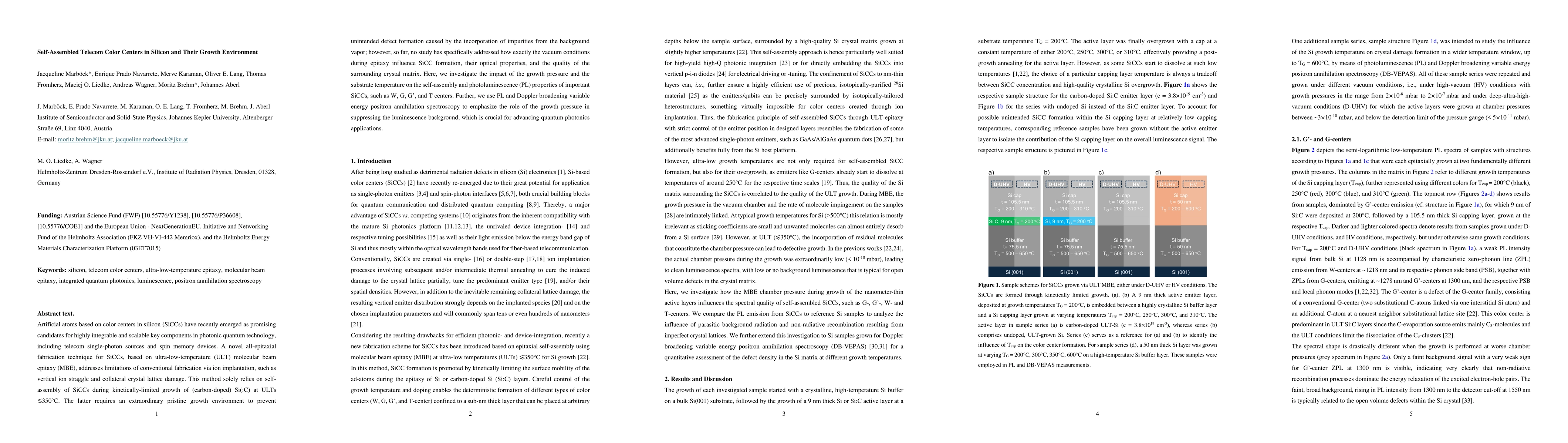
Key Findings, in focus

Seven facets of this paper, analysed and brought into focus by AI.

AI-generated · verify against source Generated Apr 09, 2026
In focus · one-line synthesis

The study provides a clear recipe for integrating telecom‑wavelength silicon color centers with minimal background, enabling scalable quantum photonic devices such as single‑photon sources and spin memories.

01
MethodologyHow they did it

All-epitaxial ULT MBE growth of carbon-doped Si layers at TG≤350 °C under varying growth pressures (HV to D‑UHV), followed by micro‑PL at 15 K and Doppler‑broadening variable‑energy positron annihilation spectroscopy to quantify defect densities.

02
ResultsWhat they found
  • Lower growth pressure (≤10⁻¹¹ mbar) and TG≤350 °C yields self‑assembled W, G, G′ and T centers with strong ZPLs while keeping the surrounding Si matrix essentially defect‑free.
  • High growth pressure (>10⁻⁸ mbar) suppresses W‑center emission, increases non‑radiative recombination, and introduces a pronounced defect‑background PL band.
  • DB‑VEPAS shows defect densities drop from ~1.1×10²⁰ cm⁻³ at 200 °C to ~1×10¹⁶ cm⁻³ at 350 °C and 600 °C, confirming that ULT growth requires D‑UHV to achieve near‑defect‑free material.
03
SignificanceWhy it matters

The study provides a clear recipe for integrating telecom‑wavelength silicon color centers with minimal background, enabling scalable quantum photonic devices such as single‑photon sources and spin memories.

04
Technical ContributionsWhat's new technically

Demonstration of kinetically‑induced self‑assembly of telecom‑wavelength silicon color centers via ULT MBE and quantitative correlation of growth pressure with defect density using PL and DB‑VEPAS.

05
NoveltyWhat sets it apart

First systematic investigation of how vacuum pressure and growth temperature jointly control color‑center formation and matrix quality in ULT silicon epitaxy, establishing D‑UHV as a prerequisite for high‑quality telecom SiCCs.

06
LimitationsWhat to be cautious about
  • Vertical position control for W‑centers is limited; most emitters reside in the capping layer rather than the intended 9 nm active layer.
  • The approach is confined to ultra‑low temperatures; higher‑temperature growth relaxes the vacuum requirement but sacrifices color‑center formation.
07
Future WorkWhere it goes next
  • Optimize the temperature differential between active and capping layers to improve vertical selectivity of W‑centers.
  • Extend the D‑UHV ULT MBE methodology to strained SiGe, Ge, and GeSn layers for next‑generation nanoelectronic and photonic applications.

Paper Details

Paper ID: 2604.06766
Comments: 25 pages, 7 Figures
Categories:
cond-mat.mes-hall physics.optics

How to Cite This Paper

Reference manager: RIS EndNote


Discussion 0

This website uses cookies to ensure you get the best experience. Learn more