Publication

Published: Apr 08, 2026
Categories: cs.AR, cs.AI

Metrics

Source: ArXiv

Quick Actions

View PDF

Quick Answers

What methodology did the authors use?

Self‑calibrating framework that uses a large language model to derive topology‑specific analytical sizing equations from a raw netlist, a one‑shot DC operating‑point calibration to extract process‑dependent parameters, and a prediction‑error feedback loop that iteratively refines the sizing function until all specifications are met. More in Methodology →

What are the key results?

All 12 OTA topology–node combinations met target specifications, converging in 2–16 simulations (median 6.5). — Convergence was driven by the measurement‑feedback architecture, not by initial prediction accuracy; even large initial errors were corrected. More in Key Results →

Why is this work significant?

Shows that LLMs can autonomously generate correct design equations from raw netlists, enabling automated, cross‑node analog sizing without training or per‑topology tuning, and providing transparent design rationale that can replace black‑box optimizers. More in Significance →

What are the main limitations?

Framework relies on fresh LLM sessions each round, which may increase simulation counts. — Accuracy depends on the extraction of four device parameters and the handling of parasitic effects; insufficient modeling can require additional rounds. More in Limitations →

Paper Preview

Abstract

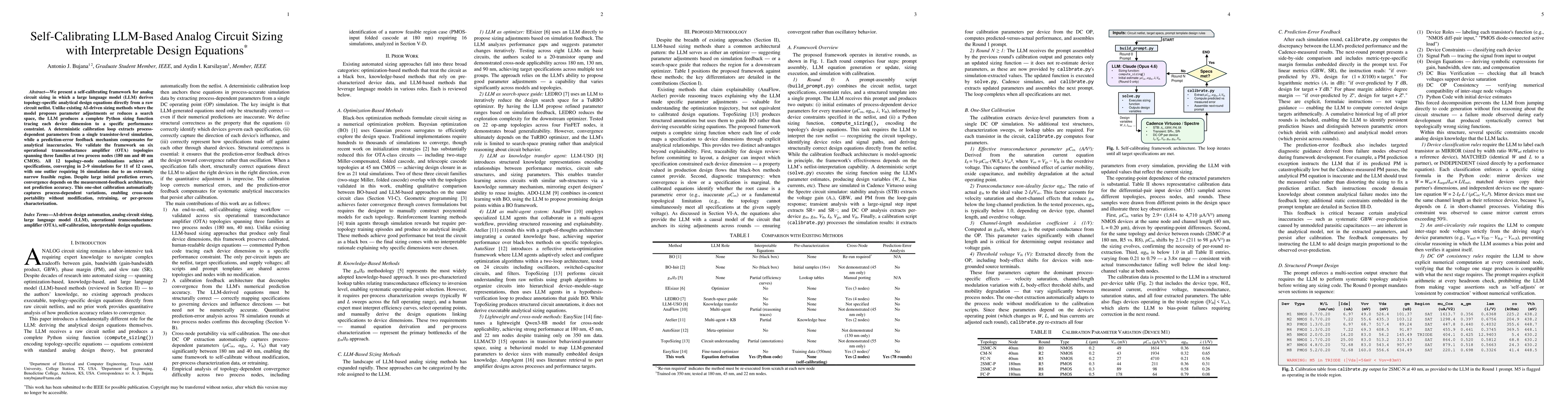
We present a self-calibrating framework for analog circuit sizing in which a large language model (LLM) derives topology-specific analytical design equations directly from a raw circuit netlist. Unlike existing AI-driven sizing methods where the model proposes parameter adjustments or reduces a search space, the LLM produces a complete Python sizing function tracing each device dimension to a specific performance constraint. A deterministic calibration loop extracts process-dependent parameters from a single transistor-level simulation, while a prediction-error feedback mechanism compensates for analytical inaccuracies. We validate the framework on six operational transconductance amplifier (OTA) topologies spanning three families at two process nodes (180 nm and 40 nm CMOS). All 12 topology-node combinations achieve all specifications, converging in 2-9 simulations for 11 of 12 cases, with one outlier requiring 16 simulations due to an extremely narrow feasible region. Despite large initial prediction errors, convergence depends on the measurement-feedback architecture, not prediction accuracy. This one-shot calibration automatically captures process-dependent variations, enabling cross-node portability without modification, retraining, or per-process characterization.

AI Key Findings

Generated Apr 12, 2026

Methodology — What approach did the authors take?

Self‑calibrating framework that uses a large language model to derive topology‑specific analytical sizing equations from a raw netlist, a one‑shot DC operating‑point calibration to extract process‑dependent parameters, and a prediction‑error feedback loop that iteratively refines the sizing function until all specifications are met.

Key Results — What are the main findings?

  • All 12 OTA topology–node combinations met target specifications, converging in 2–16 simulations (median 6.5).
  • Convergence was driven by the measurement‑feedback architecture, not by initial prediction accuracy; even large initial errors were corrected.
  • The LLM produced fully interpretable, auditable Python sizing functions with correct device‑to‑spec mapping, verified for structural correctness.

Significance — Why does this research matter?

Shows that LLMs can autonomously generate correct design equations from raw netlists, enabling automated, cross‑node analog sizing without training or per‑topology tuning, and providing transparent design rationale that can replace black‑box optimizers.

Technical Contribution — What is the technical contribution?

A self‑calibrating analog sizing system that combines LLM‑derived analytical equations, one‑shot process calibration, and prediction‑error feedback to produce interpretable, cross‑node sizing functions that converge reliably.

Novelty — What is new about this work?

First demonstration of an LLM that automatically derives topology‑specific design equations from raw netlists and uses them in an iterative calibration loop without training, yielding fully interpretable sizing functions and convergence independent of initial prediction accuracy.

Limitations — What are the limitations of this study?

  • Framework relies on fresh LLM sessions each round, which may increase simulation counts.
  • Accuracy depends on the extraction of four device parameters and the handling of parasitic effects; insufficient modeling can require additional rounds.

Future Work — What did the authors propose for future work?

  • Apply the framework to more complex, multi‑stage or mixed‑signal topologies.
  • Integrate higher‑order parasitic models or refined analytical equations to reduce prediction errors and further shorten convergence.

Paper Details

Paper ID: 2604.07387
Comments: 11 pages, 5 figures, 4 tables. Submitted to IEEE Transactions on Circuits and Systems for Artificial Intelligence (TCASAI)
Categories:
cs.AR cs.AI

How to Cite This Paper

BibTeX
@article{bujana2026self,
  title         = {Self-Calibrating LLM-Based Analog Circuit Sizing with Interpretable Design Equations},
  author        = {Bujana, Antonio J. and Karsilayan, Aydin I.},
  year          = {2026},
  eprint        = {2604.07387},
  archivePrefix = {arXiv},
  primaryClass  = {cs.AR},
}
APA 7
Bujana, A., & Karsilayan, A. (2026). Self-Calibrating LLM-Based Analog Circuit Sizing with Interpretable Design Equations. arXiv. https://arxiv.org/abs/2604.07387
MLA 9
Bujana, Antonio J., and Aydin I. Karsilayan. "Self-Calibrating LLM-Based Analog Circuit Sizing with Interpretable Design Equations." arXiv, 2026, arxiv.org/abs/2604.07387.

Comments (0)

This website uses cookies to ensure you get the best experience. Learn more