ArxivLens
ArXiv cond-mat.mtrl-sci

Self-compensation by silicon $DX$ centers in ultrawide-bandgap nitrides

Darshana Wickramaratne, John L. Lyons

2604.09842 Published Apr 10, 2026
View PDF

Publication

Published: Apr 10, 2026
Categories: cond-mat.mtrl-sci

Metrics

Source: ArXiv

Quick Answers

What methodology did the authors use?

Density functional theory calculations of Si donor transition levels combined with quasi-harmonic approximation for temperature-dependent band edges, followed by self-consistent charge neutrality to predict free carrier concentrations. More in Methodology →

What are the key results?

In AlN, the Si DX level lies ~270 meV below the CBM, causing strong compensation that limits free electron density to ~3.4×10^14 cm^−3 regardless of doping level. — Alloying with Ga (AlGaN) shifts the DX level closer to the CBM, markedly increasing donor activation and free carrier concentration, especially for light doping. More in Key Results →

Why is this work significant?

The study quantifies how Si DX centers limit n‑type conductivity in ultrawide‑bandgap nitrides, guiding material design for high‑power and high‑temperature devices. More in Significance →

What are the main limitations?

Idealized model assumes no other defects or acceptors; real samples may have additional compensation. — Short‑range order around Si dopants and alloy scattering effects are neglected, potentially affecting mobility predictions. More in Limitations →

Paper Preview

Abstract

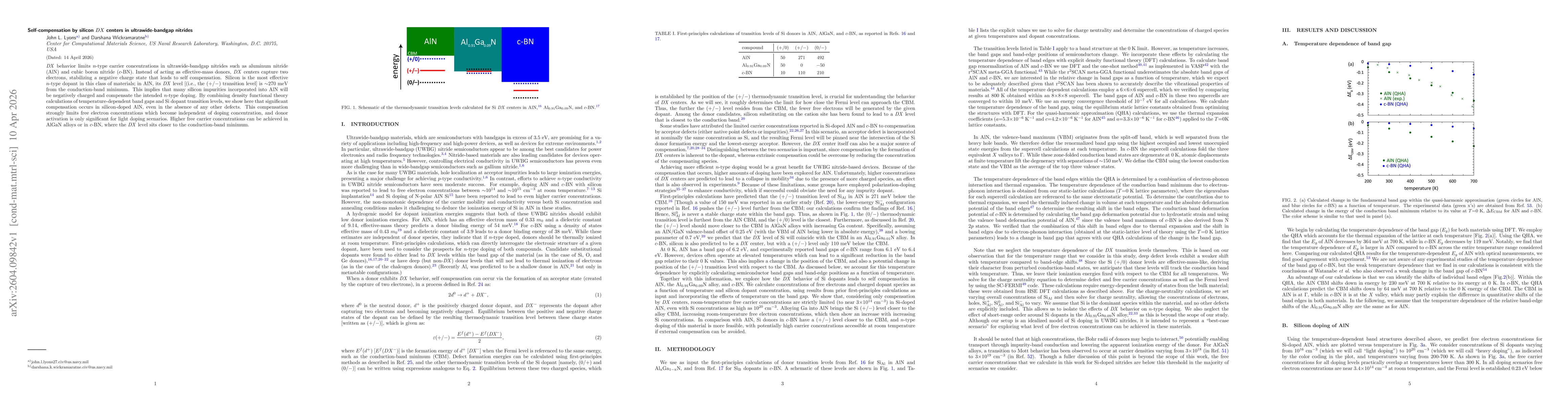
\textit{DX} behavior limits $n$-type carrier concentrations in ultrawide-bandgap nitrides such as aluminum nitride (AlN) and cubic boron nitride ($c$-BN). Instead of acting as effective-mass donors, \textit{DX} centers capture two electrons, stabilizing a negative charge state that leads to self compensation. Silicon is the most effective $n$-type dopant in this class of materials; in AlN, its \textit{DX} level [(i.e., the (+/$-$) transition level] is $\sim$270 meV from the conduction-band minimum. This implies that many silicon impurities incorporated into AlN will be negatively charged and compensate the intended $n$-type doping. By combining density functional theory calculations of temperature-dependent band gaps and Si dopant transition levels, we show here that significant compensation occurs in silicon-doped AlN, even in the absence of any other defects. This compensation strongly limits free electron concentrations which become independent of doping concentration, and donor activation is only significant for light doping scenarios. Higher free carrier concentrations can be achieved in AlGaN alloys or in $c$-BN, where the \textit{DX} level sits closer to the conduction-band minimum.

Key Findings, in focus

Seven facets of this paper, analysed and brought into focus by AI.

AI-generated · verify against source Generated Apr 15, 2026
In focus · one-line synthesis

The study quantifies how Si DX centers limit n‑type conductivity in ultrawide‑bandgap nitrides, guiding material design for high‑power and high‑temperature devices.

01
MethodologyHow they did it

Density functional theory calculations of Si donor transition levels combined with quasi-harmonic approximation for temperature-dependent band edges, followed by self-consistent charge neutrality to predict free carrier concentrations.

02
ResultsWhat they found
  • In AlN, the Si DX level lies ~270 meV below the CBM, causing strong compensation that limits free electron density to ~3.4×10^14 cm^−3 regardless of doping level.
  • Alloying with Ga (AlGaN) shifts the DX level closer to the CBM, markedly increasing donor activation and free carrier concentration, especially for light doping.
  • In cubic BN, the Si DX level is only ~110 meV below the CBM, leading to weaker compensation and higher free carrier densities (~1.5×10^17 cm^−3 at 10^20 cm^−3 doping).
03
SignificanceWhy it matters

The study quantifies how Si DX centers limit n‑type conductivity in ultrawide‑bandgap nitrides, guiding material design for high‑power and high‑temperature devices.

04
Technical ContributionsWhat's new technically

First integrated DFT and QHA framework that predicts temperature‑dependent band edges, Si DX transition levels, and self‑compensation behavior in AlN, AlGaN, and c‑BN.

05
NoveltyWhat sets it apart

Provides the first quantitative, temperature‑dependent analysis of Si DX compensation across multiple ultrawide‑bandgap nitrides, revealing that compensation limits free carriers independent of doping level.

06
LimitationsWhat to be cautious about
  • Idealized model assumes no other defects or acceptors; real samples may have additional compensation.
  • Short‑range order around Si dopants and alloy scattering effects are neglected, potentially affecting mobility predictions.
07
Future WorkWhere it goes next
  • Incorporate native defects and acceptor impurities to assess their impact on compensation.
  • Experimentally validate temperature-dependent bandgap and DX level shifts, and measure carrier mobilities in AlGaN alloys.

Paper Details

Paper ID: 2604.09842
Comments: 10 pages, 4 figures
Categories:
cond-mat.mtrl-sci

How to Cite This Paper

Reference manager: RIS EndNote


Discussion 0

This website uses cookies to ensure you get the best experience. Learn more