Publication
Metrics
Quick Actions
Abstract
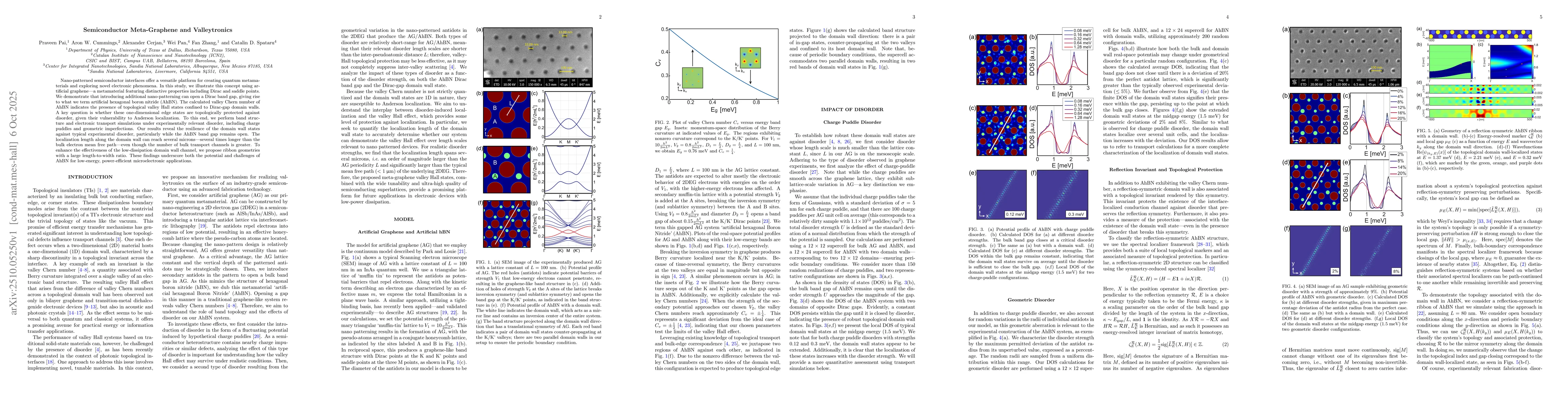
Nano-patterned semiconductor interfaces offer a versatile platform for creating quantum metamaterials and exploring novel electronic phenomena. In this study, we illustrate this concept using artificial graphene--a metamaterial featuring distinctive properties including Dirac and saddle points. We demonstrate that introducing additional nano-patterning can open a Dirac band gap, giving rise to what we term artificial hexagonal boron nitride (AhBN). The calculated valley Chern number of AhBN indicates the presence of topological valley Hall states confined to Dirac-gap domain walls. A key question is whether these one-dimensional edge states are topologically protected against disorder, given their vulnerability to Anderson localization. To this end, we perform band structure and electronic transport simulations under experimentally relevant disorder, including charge puddles and geometric imperfections. Our results reveal the resilience of the domain wall states against typical experimental disorder, particularly while the AhBN band gap remains open. The localization length along the domain wall can reach several microns--several times longer than the bulk electron mean free path--even though the number of bulk transport channels is greater. To enhance the effectiveness of the low-dissipation domain wall channel, we propose ribbon geometries with a large length-to-width ratio. These findings underscore both the potential and challenges of AhBN for low-energy, power-efficient microelectronic applications.
AI Key Findings
Generated Oct 11, 2025
Methodology
The study combines theoretical analysis with numerical simulations to investigate topological transport properties in artificial honeycomb lattices, focusing on domain wall states and their robustness against disorder.
Key Results
- Domain wall states in hexagonal boron nitride (hBN) exhibit robust topological transport with localization lengths exceeding 10 microns.
- Transport properties in narrow channels show enhanced performance of domain wall states compared to bulk hBN.
- Numerical simulations confirm the resilience of domain wall states against experimentally relevant disorder.
Significance
This research demonstrates the potential of nano-patterned materials for topological electronics, offering new avenues for designing robust quantum devices and advancing microelectronics with topological protection.
Technical Contribution
The work introduces a novel approach to analyze topological transport using spectral localizers and numerical K-theory, providing a framework for understanding and designing robust topological states in artificial materials.
Novelty
This research presents the first demonstration of designable bandgaps at the Dirac point in nano-patterned materials, enabling artificial analogs of hBN with nontrivial valley-projected band topology.
Limitations
- The study primarily focuses on idealized lattice models and may not fully capture complex real-world material imperfections.
- Transport measurements in narrow channels require advanced fabrication techniques that are currently challenging to implement.
Future Work
- Exploring the integration of domain wall-based transport in practical microelectronic devices.
- Investigating the effects of different types of disorder on topological transport properties.
- Developing scalable fabrication methods for high-aspect-ratio nanostructures.
PDF Preview
Similar Papers
Found 4 papersLight-Induced Valleytronics in Pristine Graphene
Gopal Dixit, Misha Ivanov, Álvaro Jiménez-Galán et al.
Comments (0)