Sensing Remote Bulk Defects Through Resistance Noise in a Large Area Graphene Field Effect Transistor
Publication
Metrics
AI Quick Summary
This paper investigates the impact of remote bulk defects in a lightly doped Si/SiO$_2$ substrate on the resistance noise in large area CVD graphene FETs. It reveals that charge fluctuations within the silicon substrate can be sensed by the graphene channel due to reduced screening, leading to observable noise peaks near the depletion region.
Paper Preview
Abstract
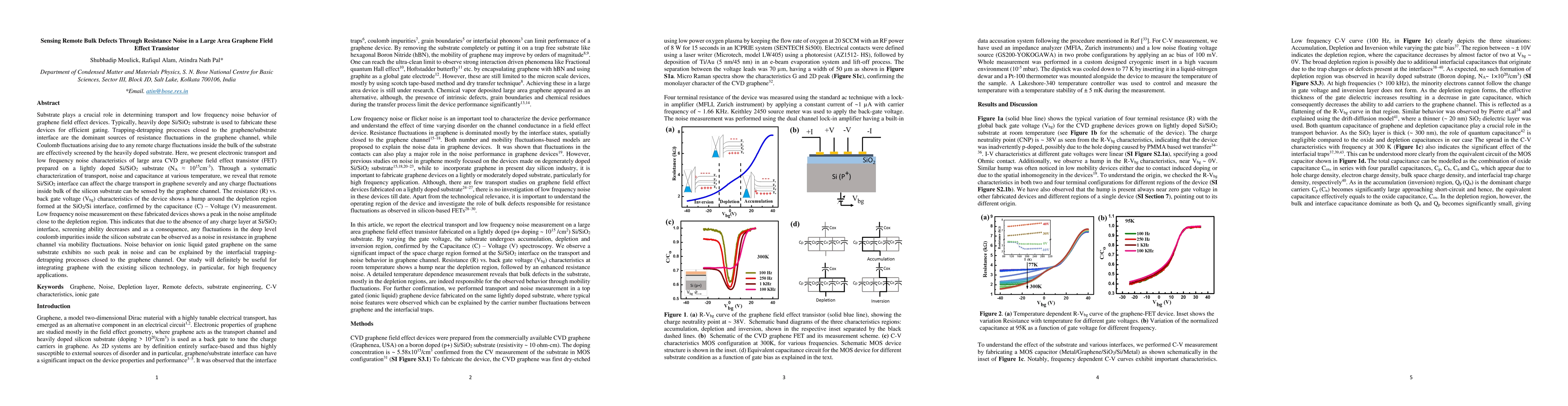
Substrate plays a crucial role in determining transport and low frequency noise behavior of graphene field effect devices. Typically, heavily dope Si/SiO$_2$ substrate is used to fabricate these devices for efficient gating. Trapping-detrapping processes closed to the graphene/substrate interface are the dominant sources of resistance fluctuations in the graphene channel, while Coulomb fluctuations arising due to any remote charge fluctuations inside the bulk of the substrate are effectively screened by the heavily doped substrate. Here, we present electronic transport and low frequency noise characteristics of large area CVD graphene field effect transistor (FET) prepared on a lightly doped Si/SiO$_2$ substrate (N$_A$ $\sim$ 10$^{15}$cm$^{-3}$). Through a systematic characterization of transport, noise and capacitance at various temperature, we reveal that remote Si/SiO$_2$ interface can affect the charge transport in graphene severely and any charge fluctuations inside bulk of the silicon substrate can be sensed by the graphene channel. The resistance (R) vs. back gate voltage (V$_{bg}$) characteristics of the device shows a hump around the depletion region formed at the SiO$_2$/Si interface, confirmed by the capacitance (C) - Voltage (V) measurement. Low frequency noise measurement on these fabricated devices shows a peak in the noise amplitude close to the depletion region. This indicates that due to the absence of any charge layer at Si/SiO$_2$ interface, screening ability decreases and as a consequence, any fluctuations in the deep level coulomb impurities inside the silicon substrate can be observed as a noise in resistance in graphene channel via mobility fluctuations. Noise behavior on ionic liquid gated graphene on the same substrate exhibits no such peak in noise and can be explained by the interfacial trapping - detrapping processes closed to the graphene channel.
AI Key Findings
Get AI-generated insights about this paper's methodology, results, significance, and more — seven facets brought into focus.
Impact
Paper Details
Authors
PDF Preview
Key Terms
Citation Network
Current paper (gray), citations (green), references (blue)
Display is limited for performance on very large graphs.
Discussion 0