01
MethodologyHow they did it
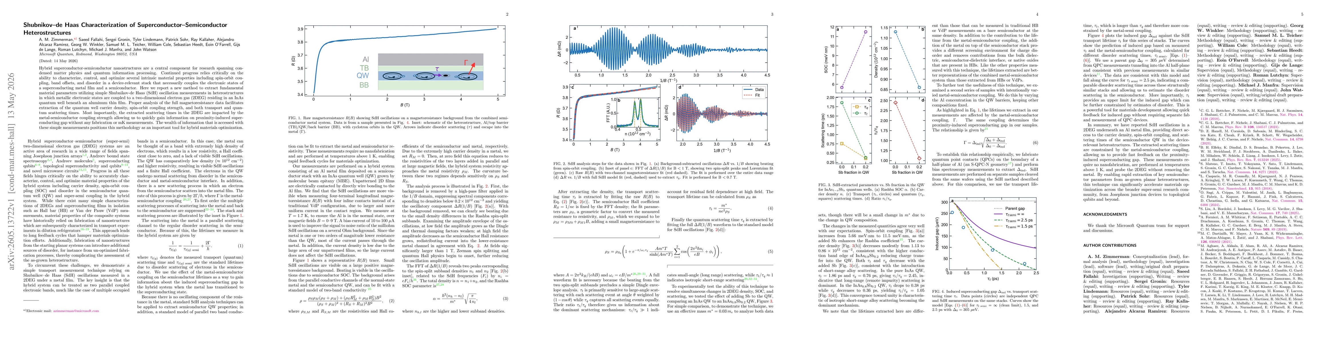
The study uses Shubnikov–de Haas oscillations in a planar Al/InAs heterostructure to extract semiconductor quantum well parameters. By analyzing the full magnetoresistance with high-pass filtering in 1/B to isolate oscillatory components, the authors decode two Rashba-split subbands, obtain carrier densities, and determine spin-orbit coupling strength. They model the total hybrid resistivity as parallel conduction of the semiconductor QW and the metal film, and relate measured transport lifetimes to scattering processes including metal–semiconductor coupling via 1/τt(q)=1/τt(q)semi+2Γ/ℏ, enabling estimation of proximity-induced superconducting gap without low-temperature fabrication steps.
Discussion 0