01
MethodologyHow they did it
High magnetic field and low temperature transport measurements are conducted on 2D PtSe2 to investigate its charge carriers.
Researchers investigate 2D PtSe2 material using high magnetic fields and low temperatures, revealing Shubnikov-de Haas oscillations that provide insights into the material's charge carriers and transport properties.
Researchers investigate 2D PtSe2 material using high magnetic fields and low temperatures, revealing Shubnikov-de Haas oscillations that provide insights into the material's charge carriers and transport properties.
High magnetic field and low temperature transport measurements are conducted on 2D PtSe2 to investigate its charge carriers. More in Methodology →
Shubnikov-de Haas oscillations occur exclusively in plane for magnetic fields ≥ 4.5 T. — Oscillations emerge at a layer thickness of ~18 nm, with amplitude increasing and frequency decreasing for thinner flakes. More in Key Results →
Provides detailed understanding of charge carriers and transport phenomena in PtSe2, crucial for spintronic and orbitronic device design, as well as realization of orbital Hall effect-based architectures. More in Significance →
Limited to 2D PtSe2; results may not generalize to other materials or dimensions. — Experimental constraints may affect the precise determination of certain transport parameters. More in Limitations →
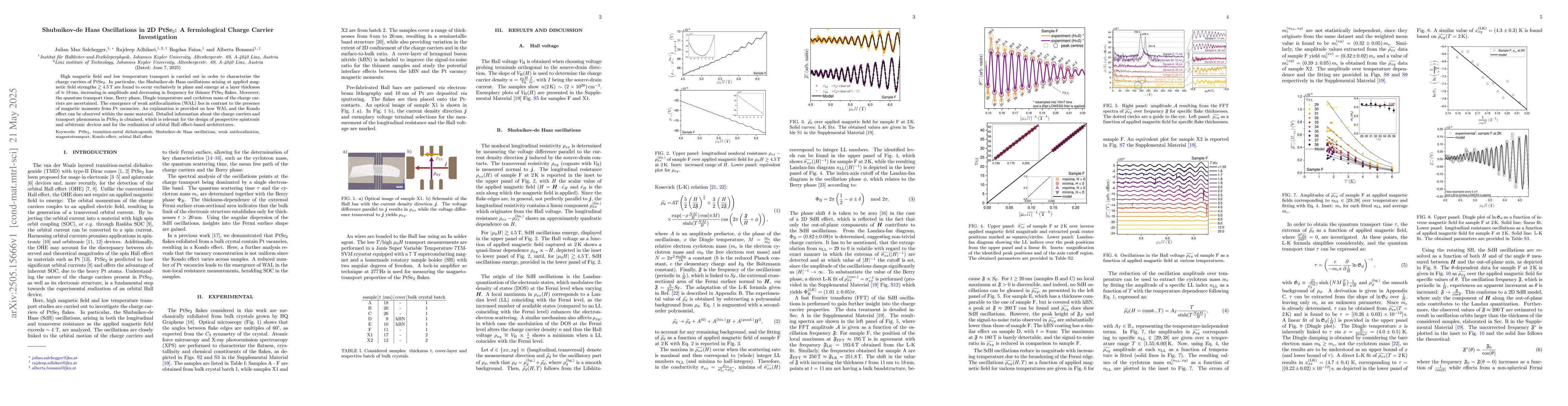
High magnetic field and low temperature transport is carried out in order to characterize the charge carriers of $\text{PtSe}_2$. In particular, the Shubnikov-de Haas oscillations arising at applied magnetic field strengths $\gtrsim 4.5\,\text{T}$ are found to occur exclusively in plane and emerge at a layer thickness of $\approx 18\,\text{nm}$, increasing in amplitude and decreasing in frequency for thinner $\text{PtSe}_2$ flakes. Moreover, the quantum transport time, Berry phase, Dingle temperature and cyclotron mass of the charge carriers are ascertained. The emergence of weak antilocalization (WAL) lies in contrast to the presence of magnetic moments from Pt vacancies. An explanation is provided on how WAL and the Kondo effect can be observed within the same material. Detailed information about the charge carriers and transport phenomena in $\text{PtSe}_2$ is obtained, which is relevant for the design of prospective spintronic and orbitronic devices and for the realization of orbital Hall effect-based architectures.
Seven facets of this paper, analysed and brought into focus by AI.
Provides detailed understanding of charge carriers and transport phenomena in PtSe2, crucial for spintronic and orbitronic device design, as well as realization of orbital Hall effect-based architectures.
High magnetic field and low temperature transport measurements are conducted on 2D PtSe2 to investigate its charge carriers.
Provides detailed understanding of charge carriers and transport phenomena in PtSe2, crucial for spintronic and orbitronic device design, as well as realization of orbital Hall effect-based architectures.
Detailed characterization of charge carrier behavior in 2D PtSe2 under high magnetic fields, including determination of transport parameters and observation of WAL.
Demonstrates coexistence of weak antilocalization and Kondo effect in the same material, offering insights into complex quantum transport phenomena in 2D materials.
Current paper (gray), citations (green), references (blue)
Display is limited for performance on very large graphs.
Discussion 0