Publication
Metrics
AI Quick Summary
This paper details the signal generation mechanism in CdTe semiconductor sensors, deriving fundamental semiconductor relations and focusing on Schottky-type CdTe:Cl sensors used in the STIX instrument on the ESA Solar Orbiter mission. The analysis is broadly applicable to various semiconductors.
Paper Preview
Abstract
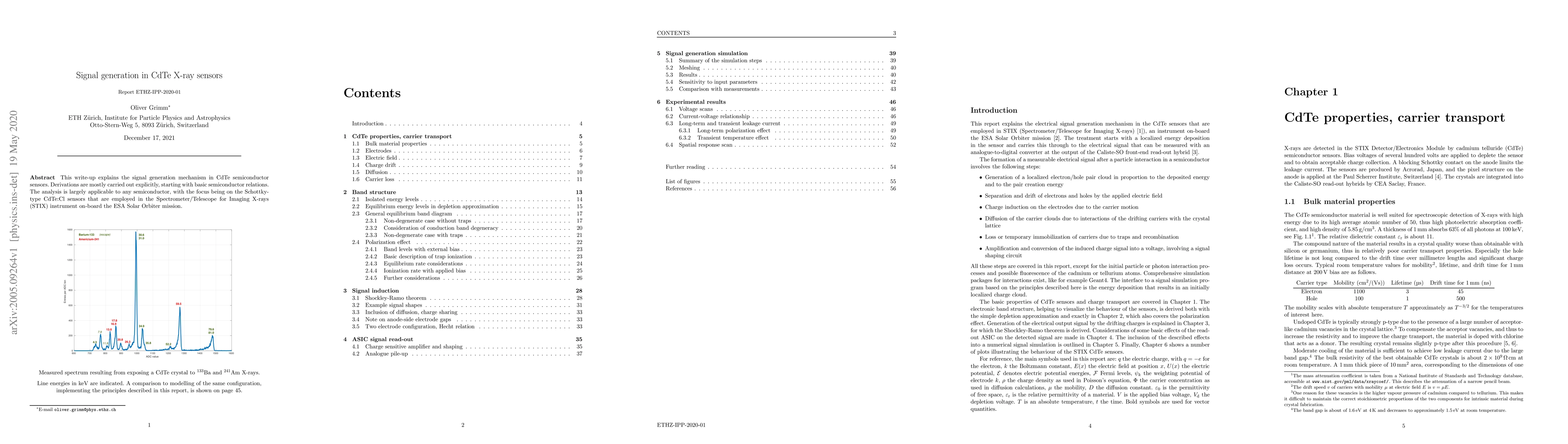
This write-up explains the signal generation mechanism in CdTe semiconductor sensors. Derivations are mostly carried out explicitly, starting with basic semiconductor relations. The analysis is largely applicable to any semiconductor, with the focus being on the Schottky-type CdTe:Cl sensors that are employed in the Spectrometer/Telescope for Imaging X-rays (STIX) instrument on-board the ESA Solar Orbiter mission.
AI Key Findings
Get AI-generated insights about this paper's methodology, results, significance, and more — seven facets brought into focus.
Impact
Paper Details
Authors
PDF Preview
Key Terms
Citation Network
Current paper (gray), citations (green), references (blue)
Display is limited for performance on very large graphs.
Discussion 0