Silicide-based Josephson field effect transistors for superconducting qubits
Publication
Metrics
AI Quick Summary
This paper explores the use of silicide-based Josephson Field-Effect Transistors (JFETS) for scalable superconducting qubits, focusing on materials like V3Si and PtSi. Experimental results on PtSi transistors demonstrate gate-modulated transparency at superconducting/semiconducting interfaces, showing Andreev current at zero bias, which is a significant step towards CMOS-integrated quantum computing.
Paper Preview
Abstract
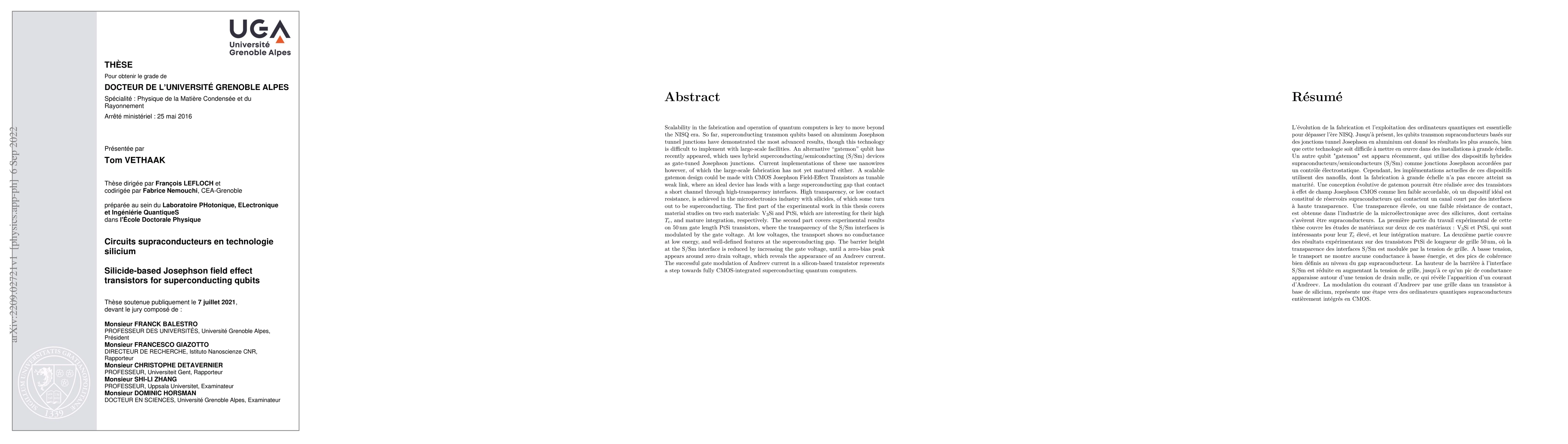
Scalability in the fabrication and operation of quantum computers is key to move beyond the NISQ era. So far, superconducting transmon qubits based on aluminum Josephson tunnel junctions have demonstrated the most advanced results, though this technology is difficult to implement with large-scale facilities. An alternative "gatemon" qubit has recently appeared, which uses hybrid superconducting/semiconducting (S/Sm) devices as gate-tuned Josephson junctions. Current implementations of these use nanowires however, of which the large-scale fabrication has not yet matured either. A scalable gatemon design could be made with CMOS Josephson Field-Effect Transistors as tunable weak link, where an ideal device has leads with a large superconducting gap that contact a short channel through high-transparency interfaces. High transparency, or low contact resistance, is achieved in the microelectronics industry with silicides, of which some turn out to be superconducting. The first part of the experimental work in this thesis covers material studies on two such materials: $\text{V}_3\text{Si}$ and PtSi, which are interesting for their high $T_\text{c}$, and mature integration, respectively. The second part covers experimental results on 50 nm gate length PtSi transistors, where the transparency of the S/Sm interfaces is modulated by the gate voltage. At low voltages, the transport shows no conductance at low energy, and well-defined features at the superconducting gap. The barrier height at the S/Sm interface is reduced by increasing the gate voltage, until a zero-bias peak appears around zero drain voltage, which reveals the appearance of an Andreev current. The successful gate modulation of Andreev current in a silicon-based transistor represents a step towards fully CMOS-integrated superconducting quantum computers.
OpenAlex
- Citations in OpenAlex
- 4
- Publication year
- 2022
- Access status
- Open access
Source: OpenAlex · Snapshot
AI Key Findings
Get AI-generated insights about this paper's methodology, results, significance, and more — seven facets brought into focus.
Paper Details
Authors
PDF Preview
Key Terms
Citation Network
Current paper (gray), citations (green), references (blue)
Display is limited for performance on very large graphs.
Related Papers
No references found for this paper.
Discussion 0