Simulation on the Miniaturization and Performance Improvement Study of Gr/MoS2 Based Vertical Field Effect Transistor
Publication
Metrics
AI Quick Summary
This paper investigates the simulation of a vertical field effect transistor (VFET) utilizing graphene (Gr) and molybdenum disulfide (MoS2) to enhance miniaturization and performance. Modifications including insulating part of the source electrode and adding a buried MoS2 layer improve the OFF current, achieving a peak ON/OFF ratio of 109, supporting low voltage operation and high switching speed in 2D material-based VFETs.
Paper Preview
Abstract
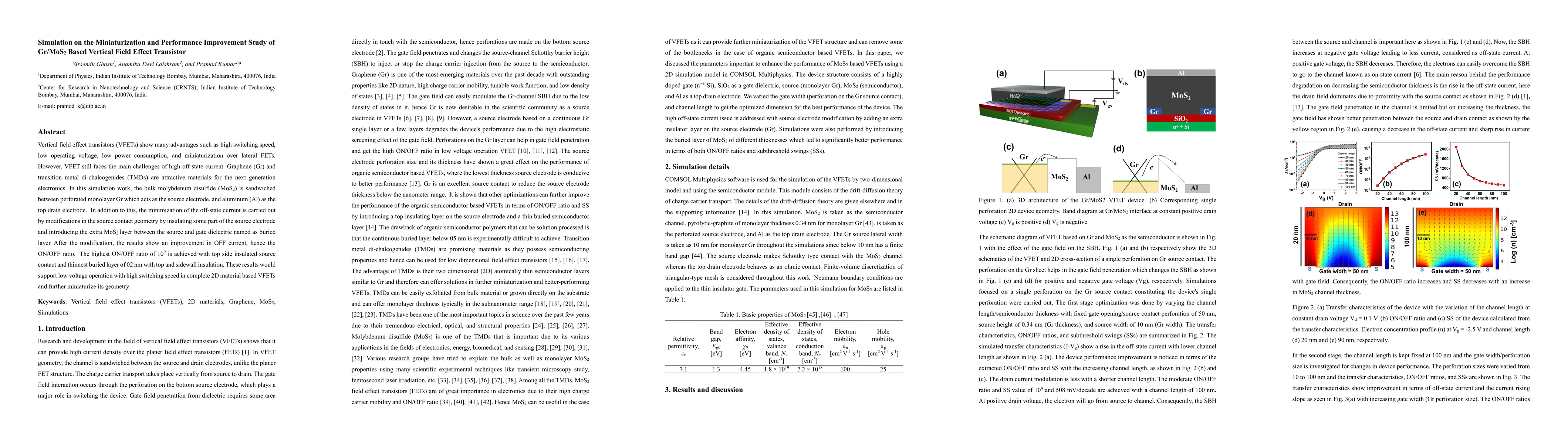
Vertical field effect transistors (VFETs) show many advantages such as high switching speed, low operating voltage, low power consumption, and miniaturization over lateral FETs. However, VFET still faces the main challenges of high off-state current. Graphene (Gr) and transition metal di-chalcogenides (TMDs) are attractive materials for the next generation electronics. In this simulation work, the bulk molybdenum disulfide (MoS2) is sandwiched between perforated monolayer Gr which acts as the source electrode, and aluminum (Al) as the top drain electrode. In addition to this, the minimization of the off-state current is carried out by modifications in the source contact geometry by insulating some part of the source electrode and introducing the extra MoS2 layer between the source and gate dielectric named as buried layer. After the modification, the results show an improvement in OFF current, hence the ON/OFF ratio. The highest ON/OFF ratio of 109 is achieved with top side insulated source contact and thinnest buried layer of 02 nm with top and sidewall insulation. These results would support low voltage operation with high switching speed in complete 2D material based VFETs and further miniaturize its geometry.
AI Key Findings
Get AI-generated insights about this paper's methodology, results, significance, and more — seven facets brought into focus.
Impact
Paper Details
Authors
PDF Preview
Citation Network
Current paper (gray), citations (green), references (blue)
Display is limited for performance on very large graphs.
Discussion 0