Publication

Published: Dec 09, 2010
Categories: cond-mat.mes-hall

Metrics

Source: ArXiv

Quick Actions

View PDF

AI Quick Summary

This paper describes a single-gate accumulation-mode InGaAs quantum dot with a vertically integrated charge sensor, achieving high DC sensitivity to single electrons and measuring state lifetimes via random telegraph signals. The device uses a double-quantum-well design and a quantum point contact for electron tunneling detection.

Quick Answers

What is "Single-Gate Accumulation-Mode InGaAs Quantum Dot with a Vertically Integrated Charge Sensor" about?

This paper describes a single-gate accumulation-mode InGaAs quantum dot with a vertically integrated charge sensor, achieving high DC sensitivity to single electrons and measuring state lifetimes via random telegraph signals. The device uses a double-quantum-well design and a quantum point contact for electron tunneling detection.

What methodology did the authors use?

The research describes the fabrication and characterization of a single-gate accumulation-mode InGaAs quantum dot integrated with a vertically aligned charge sensor using a double-quantum-well design. The device utilizes a small air-bridged gate for lateral confinement of electrons and a QPC for charge detection. More in Methodology →

What are the key results?

A few-electron quantum dot was successfully controlled by a single gate electrode with a high DC sensitivity to single electrons (8.6%). — A signal-to-noise ratio of ~9:1 and an equivalent noise bandwidth of 12.1 kHz were achieved. More in Key Results →

Why is this work significant?

This research presents a practical realization of a novel device geometry for semi-conductor quantum dots, integrating the quantum dot and readout channel vertically. It simplifies dot control and offers potential advantages over existing designs, such as easier placement of dots in close proximity and control of their coupling through an additional surface gate. More in Significance →

What are the main limitations?

The study was conducted at temperatures below 300 mK, which may limit immediate practical applications requiring higher operating temperatures. — The research did not explore the scalability of the design for larger quantum dot arrays. More in Limitations →

Paper Preview

Abstract

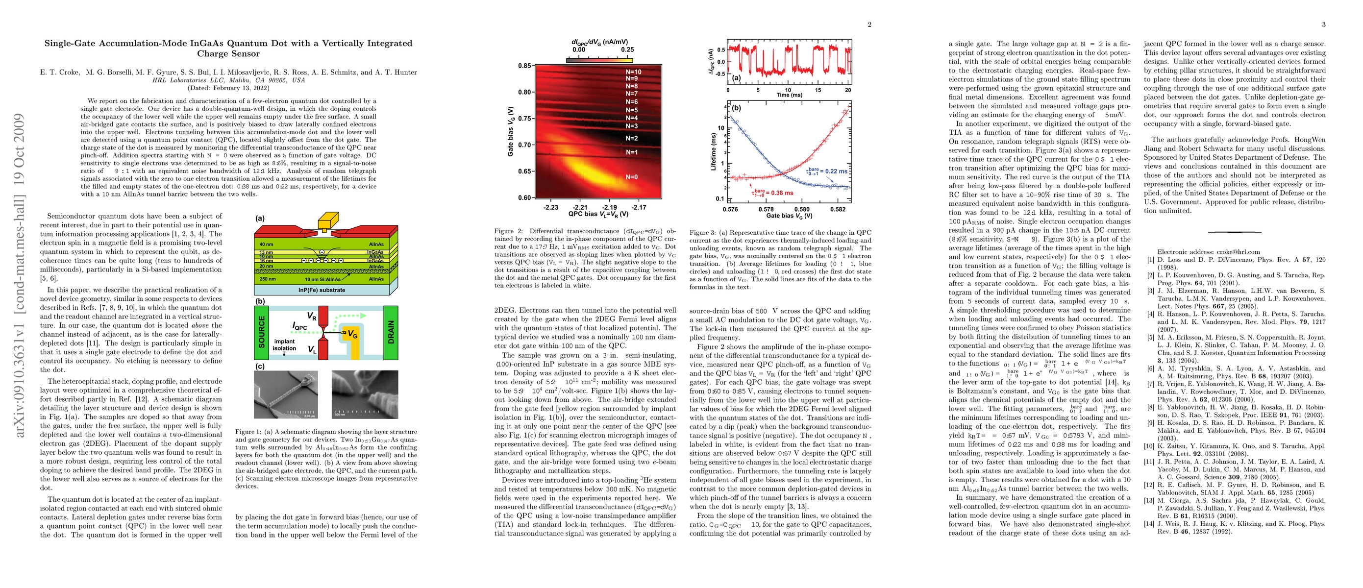
We report on the fabrication and characterization of a few-electron quantum dot controlled by a single gate electrode. Our device has a double-quantum-well design, in which the doping controls the occupancy of the lower well while the upper well remains empty under the free surface. A small air-bridged gate contacts the surface, and is positively biased to draw laterally confined electrons into the upper well. Electrons tunneling between this accumulation-mode dot and the lower well are detected using a quantum point contact (QPC), located slightly offset from the dot gate. The charge state of the dot is measured by monitoring the differential transconductance of the QPC near pinch-off. Addition spectra starting with N=0 were observed as a function of gate voltage. DC sensitivity to single electrons was determined to be as high as 8.6%, resulting in a signal-to-noise ratio of ~9:1 with an equivalent noise bandwidth of 12.1 kHz. Analysis of random telegraph signals associated with the zero to one electron transition allowed a measurement of the lifetimes for the filled and empty states of the one-electron dot: 0.38 ms and 0.22 ms, respectively, for a device with a 10 nm AlInAs tunnel barrier between the two wells.

AI Key Findings

Generated Sep 01, 2025

Methodology — What approach did the authors take?

The research describes the fabrication and characterization of a single-gate accumulation-mode InGaAs quantum dot integrated with a vertically aligned charge sensor using a double-quantum-well design. The device utilizes a small air-bridged gate for lateral confinement of electrons and a QPC for charge detection.

Key Results — What are the main findings?

  • A few-electron quantum dot was successfully controlled by a single gate electrode with a high DC sensitivity to single electrons (8.6%).
  • A signal-to-noise ratio of ~9:1 and an equivalent noise bandwidth of 12.1 kHz were achieved.
  • Lifetimes for the filled and empty states of the one-electron dot were measured: 0.38 ms for filling and 0.22 ms for emptying.
  • The design offers simplicity, as it uses a single gate electrode to define and control the dot's occupancy without requiring additional tunability of the dot.
  • The heteroepitaxial stack, doping profile, and electrode layout were optimized for desired band profiles.

Significance — Why does this research matter?

This research presents a practical realization of a novel device geometry for semi-conductor quantum dots, integrating the quantum dot and readout channel vertically. It simplifies dot control and offers potential advantages over existing designs, such as easier placement of dots in close proximity and control of their coupling through an additional surface gate.

Technical Contribution — What is the technical contribution?

The paper presents a single-gate accumulation-mode InGaAs quantum dot with a vertically integrated charge sensor, demonstrating high sensitivity to single-electron charging events and providing a simple, integrated design for quantum dot control and readout.

Novelty — What is new about this work?

This work introduces a novel vertical integration design for quantum dots with a single-gate control mechanism, offering simplicity and potential advantages over existing laterally-depleted quantum dot designs, particularly in terms of dot placement and coupling control.

Limitations — What are the limitations of this study?

  • The study was conducted at temperatures below 300 mK, which may limit immediate practical applications requiring higher operating temperatures.
  • The research did not explore the scalability of the design for larger quantum dot arrays.

Future Work — What did the authors propose for future work?

  • Investigate the device's performance at higher temperatures for practical applications.
  • Explore the scalability of the design for multi-quantum-dot systems and quantum information processing architectures.

Paper Details

Paper ID: 0910.3631
Journal: Appl. Phys. Lett. Vol. 96, 042101 (2010)
License: http://arxiv.org/licenses/nonexclusive-distrib/1.0/
Comments: 3 pages, 3 figures
Categories:
cond-mat.mes-hall

How to Cite This Paper

BibTeX
@article{anon2010single,
  title         = {Single-Gate Accumulation-Mode InGaAs Quantum Dot with a Vertically
  Integrated Charge Sensor},
  year          = {2010},
  eprint        = {0910.3631},
  archivePrefix = {arXiv},
  primaryClass  = {cond-mat.mes-hall},
  doi           = {10.1063/1.3280368},
}
APA 7
(2010). Single-Gate Accumulation-Mode InGaAs Quantum Dot with a Vertically
  Integrated Charge Sensor. arXiv. https://doi.org/10.1063/1.3280368
MLA 9
"Single-Gate Accumulation-Mode InGaAs Quantum Dot with a Vertically
  Integrated Charge Sensor." arXiv, 2010, doi.org/10.1063/1.3280368.

Key Terms

dot (0.287)
gate (0.268)
ms (0.207)
electrons (0.197)
device (0.175)
electron (0.169)
upper (0.142)
noise (0.137)

Citation Network

Current paper (gray), citations (green), references (blue)

Display is limited for performance on very large graphs.

Current Paper
Citations
References
Click to view
Title Authors Year Actions

Comments (0)

This website uses cookies to ensure you get the best experience. Learn more