Single-hole tunneling through a two-dimensional hole gas in intrinsic silicon
Publication
Metrics
Paper Preview
Abstract
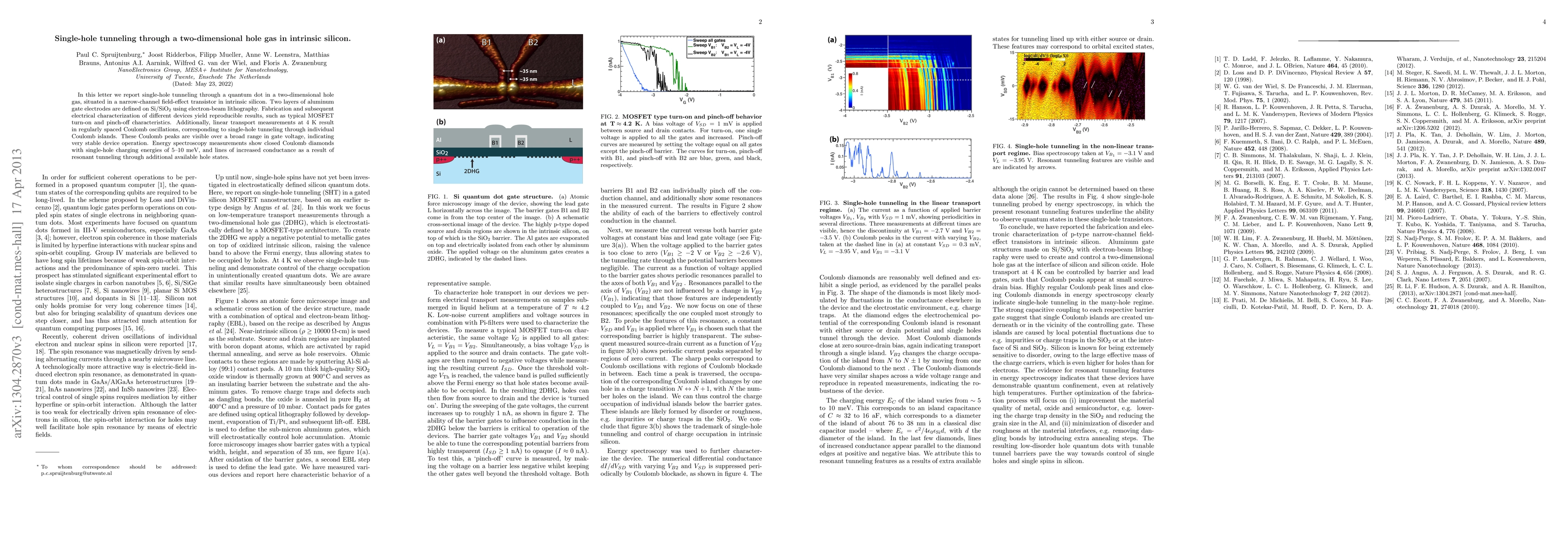
In this letter we report single-hole tunneling through a quantum dot in a two-dimensional hole gas, situated in a narrow-channel field-effect transistor in intrinsic silicon. Two layers of aluminum gate electrodes are defined on Si/SiO$_2$ using electron-beam lithography. Fabrication and subsequent electrical characterization of different devices yield reproducible results, such as typical MOSFET turn-on and pinch-off characteristics. Additionally, linear transport measurements at 4 K result in regularly spaced Coulomb oscillations, corresponding to single-hole tunneling through individual Coulomb islands. These Coulomb peaks are visible over a broad range in gate voltage, indicating very stable device operation. Energy spectroscopy measurements show closed Coulomb diamonds with single-hole charging energies of 5--10 meV, and lines of increased conductance as a result of resonant tunneling through additional available hole states.
AI Key Findings
Get AI-generated insights about this paper's methodology, results, significance, and more — seven facets brought into focus.
Impact
Paper Details
PDF Preview
Key Terms
Citation Network
Current paper (gray), citations (green), references (blue)
Display is limited for performance on very large graphs.
Discussion 0