Site-Controlled Purcell-Induced Bright Single Photon Emitters in Hexagonal Boron Nitride
Publication
Metrics
AI Quick Summary
This research demonstrates large-area arrays of plasmonic nanoresonators in hexagonal boron nitride to enhance single photon emitters' radiative emission at room temperature, achieving a five-fold reduction in decay times and a high emission rate. The architecture, featuring gold-coated silicon pillars with an alumina spacer, optimizes emitter-cavity coupling and improves quantum information system scalability.
Paper Preview
Abstract
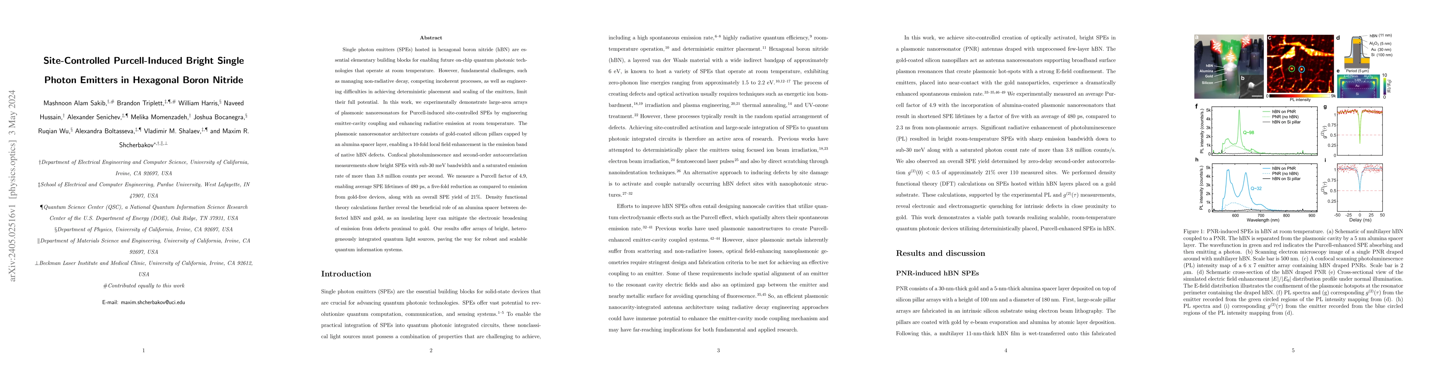
Single photon emitters (SPEs) hosted in hexagonal boron nitride (hBN) are essential elementary building blocks for enabling future on-chip quantum photonic technologies that operate at room temperature. However, fundamental challenges, such as managing non-radiative decay, competing incoherent processes, as well as engineering difficulties in achieving deterministic placement and scaling of the emitters, limit their full potential. In this work, we experimentally demonstrate large-area arrays of plasmonic nanoresonators for Purcell-induced site-controlled SPEs by engineering emitter-cavity coupling and enhancing radiative emission at room temperature. The plasmonic nanoresonator architecture consists of gold-coated silicon pillars capped with an alumina spacer layer, enabling a 10-fold local field enhancement in the emission band of native hBN defects. Confocal photoluminescence and second-order autocorrelation measurements show bright SPEs with sub-30 meV bandwidth and a saturated emission rate of more than 3.8 million counts per second. We measure a Purcell factor of 4.9, enabling average SPE lifetimes of 480 ps, a five-fold reduction as compared to emission from gold-free devices, along with an overall SPE yield of 21%. Density functional theory calculations further reveal the beneficial role of an alumina spacer between defected hBN and gold, as an insulating layer can mitigate the electronic broadening of emission from defects proximal to gold. Our results offer arrays of bright, heterogeneously integrated quantum light sources, paving the way for robust and scalable quantum information systems.
AI Key Findings
Get AI-generated insights about this paper's methodology, results, significance, and more — seven facets brought into focus.
Impact
Paper Details
Authors
PDF Preview
Key Terms
Citation Network
Current paper (gray), citations (green), references (blue)
Display is limited for performance on very large graphs.
Discussion 0