Spatially controlled electrostatic doping in graphene p-i-n junction for hybrid silicon photodiode
Publication
Metrics
AI Quick Summary
This paper presents a graphene-silicon p-i-n junction photodiode in a photonic crystal waveguide, achieving zero-bias, ultrafast photodetection with high signal-to-noise ratio. The graphene enhances device speed and efficiency through rapid carrier transfer and built-in electric field-assisted collection, marking the first post-fabrication-free integration of 2D materials in silicon photonic devices.
Paper Preview
Abstract
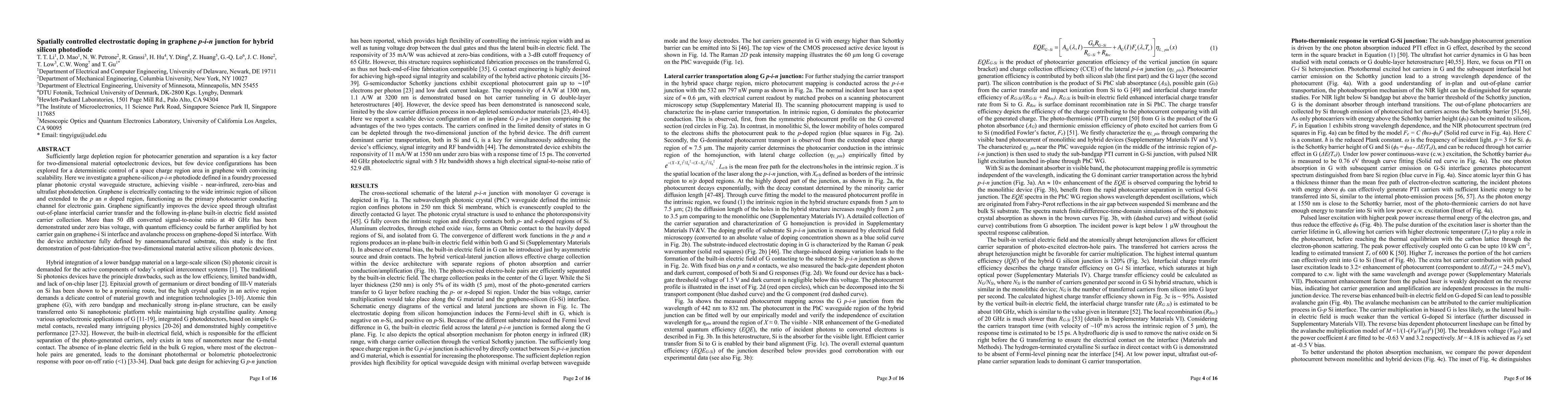
Sufficiently large depletion region for photocarrier generation and separation is a key factor for two-dimensional material optoelectronic devices, but few device configurations has been explored for a deterministic control of a space charge region area in graphene with convincing scalability. Here we investigate a graphene-silicon p-i-n photodiode defined in a foundry processed planar photonic crystal waveguide structure, achieving visible - near-infrared, zero-bias and ultrafast photodetection. Graphene is electrically contacting to the wide intrinsic region of silicon and extended to the p an n doped region, functioning as the primary photocarrier conducting channel for electronic gain. Graphene significantly improves the device speed through ultrafast out-of-plane interfacial carrier transfer and the following in-plane built-in electric field assisted carrier collection. More than 50 dB converted signal-to-noise ratio at 40 GHz has been demonstrated under zero bias voltage, with quantum efficiency could be further amplified by hot carrier gain on graphene-i Si interface and avalanche process on graphene-doped Si interface. With the device architecture fully defined by nanomanufactured substrate, this study is the first demonstration of post-fabrication-free two-dimensional material active silicon photonic devices.
AI Key Findings
Get AI-generated insights about this paper's methodology, results, significance, and more — seven facets brought into focus.
Impact
Paper Details
PDF Preview
Key Terms
Citation Network
Current paper (gray), citations (green), references (blue)
Display is limited for performance on very large graphs.
Discussion 0