Spatially-Resolved Band Gap and Dielectric Function in 2D Materials from Electron Energy Loss Spectroscopy
Publication
Metrics
AI Quick Summary
Researchers developed a method to analyze 2D materials at the nanoscale using electron energy-loss spectroscopy, revealing their band gaps and dielectric functions with unprecedented spatial resolution.
Paper Preview
Abstract
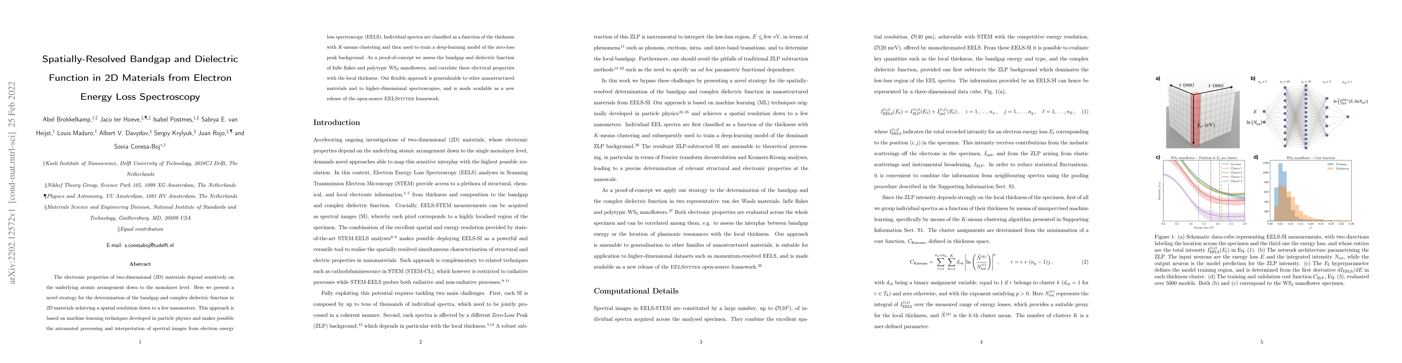
The electronic properties of two-dimensional (2D) materials depend sensitively on the underlying atomic arrangement down to the monolayer level. Here we present a novel strategy for the determination of the band gap and complex dielectric function in 2D materials achieving a spatial resolution down to a few nanometers. This approach is based on machine learning techniques developed in particle physics and makes possible the automated processing and interpretation of spectral images from electron energy-loss spectroscopy (EELS). Individual spectra are classified as a function of the thickness with $K$-means clustering and then used to train a deep-learning model of the zero-loss peak background. As a proof-of-concept we assess the band gap and dielectric function of InSe flakes and polytypic WS$_2$ nanoflowers, and correlate these electrical properties with the local thickness. Our flexible approach is generalizable to other nanostructured materials and to higher-dimensional spectroscopies, and is made available as a new release of the open-source EELSfitter framework.
AI Key Findings
Get AI-generated insights about this paper's methodology, results, significance, and more — seven facets brought into focus.
Impact
Paper Details
Authors
PDF Preview
Key Terms
Citation Network
Current paper (gray), citations (green), references (blue)
Display is limited for performance on very large graphs.
Discussion 0