Quick Summary:

This paper investigates the electronic properties of single-layer WS$_2$ on high-$\kappa$ transition metal oxide substrates, finding that the material's electronic structure remains consistent with predictions, indicating strong spin-orbit coupling and a direct band gap. The results suggest potential for combining TMDCs with various oxides to control optoelectronic properties.

Summary

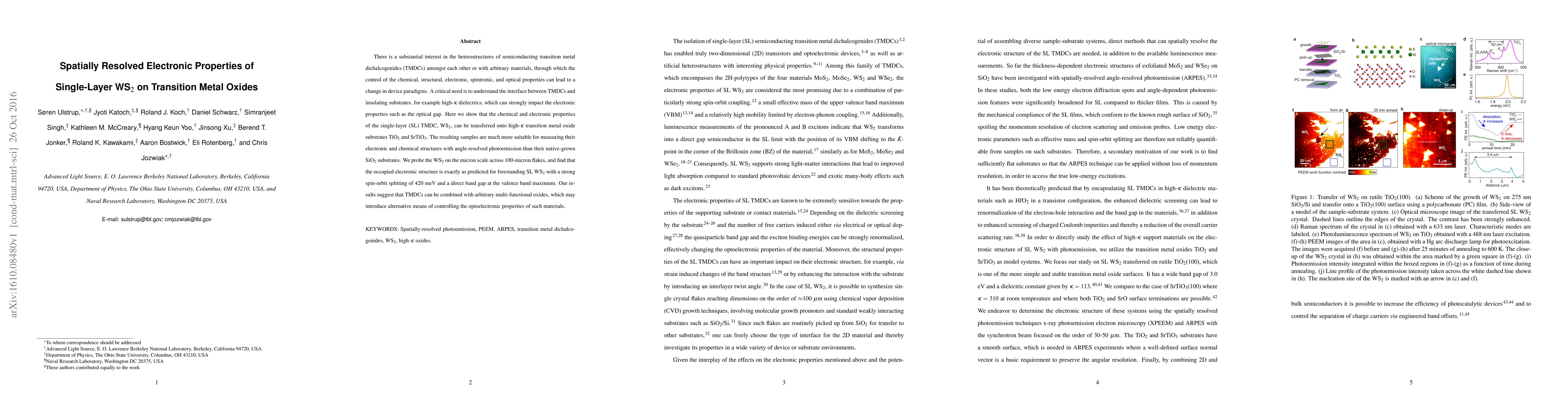
There is a substantial interest in the heterostructures of semiconducting transition metal dichalcogenides (TMDCs) amongst each other or with arbitrary materials, through which the control of the chemical, structural, electronic, spintronic, and optical properties can lead to a change in device paradigms. A critical need is to understand the interface between TMDCs and insulating substrates, for example high-$\kappa$ dielectrics, which can strongly impact the electronic properties such as the optical gap. Here we show that the chemical and electronic properties of the single-layer (SL) TMDC, WS$_2$, can be transferred onto high-$\kappa$ transition metal oxide substrates TiO$_2$ and SrTiO$_3$. The resulting samples are much more suitable for measuring their electronic and chemical structures with angle-resolved photoemission than their native-grown SiO$_2$ substrates. We probe the WS$_2$ on the micron scale across 100-micron flakes, and find that the occupied electronic structure is exactly as predicted for freestanding SL WS$_2$ with a strong spin-orbit splitting of 420~meV and a direct band gap at the valence band maximum. Our results suggest that TMDCs can be combined with arbitrary multi-functional oxides, which may introduce alternative means of controlling the optoelectronic properties of such materials.

AI Key Findings

Get AI-generated insights about this paper's methodology, results, and significance.

Paper Details

PDF Preview

Download PDF

Key Terms

_2 (0.261)
substrates (0.255)
electronic (0.236)
micron (0.208)
transition metal (0.206)
sl (0.198)
kappa (0.197)
chemical (0.188)
metal (0.156)
materials (0.144)
band (0.141)
properties (0.136)
arbitrary (0.134)
gap (0.133)
oxide (0.126)
oxides (0.126)
optical (0.125)
spintronic (0.123)
band gap (0.123)
insulating (0.123)
Title Authors Year Actions
Exchange-enhanced spin-orbit splitting and its density dependence for electrons in monolayer transition metal dichalcogenides
Igor Rozhansky, V. Fal’ko
2024
View Paper
Investigation of Strain Modulated Opto-Electronic Properties in Monolayer WX2 (X = Se and S): DFT and Beyond DFT Study
Ahsan Javed, Muhammad Asif, Rafi Ullah
2024
View Paper
Berry curvature signatures in chiroptical excitonic transitions
S. Beaulieu, S. Dong, Viktor Christiansson, P. Werner, T. Pincelli, J. Ziegler, T. Taniguchi, Kenji Watanabe, A. Chernikov, M. Wolf, L. Rettig, R. Ernstorfer, Michael Schüler
2023
View Paper
Band structure and spin texture of 2D materials for valleytronics: insights from spin and angle-resolved photoemission spectroscopy
F. Bussolotti, T. D. Maddumapatabandi, K. Goh
2023
View Paper
Development of in situ characterization of two-dimensional materials grown on insulator substrates with spectroscopic photoemission and low energy electron microscopy
Guanhua Zhang, Lina Liu, Shengxue Zhou, Y. Liang, Julong Sun, Lei Liu, Chuanyao Zhou, Liying Jiao, Xueming Yang, Zefeng Ren
2023
View Paper
Laser-Patterned Submicrometer Bi2Se3-WS2 Pixels with Tunable Circular Polarization at Room Temperature.
Zachariah Hennighausen, D. Wickramaratne, K. McCreary, B. Hudak, T. Brintlinger, Hsun-Jen Chuang, M. Noyan, B. Jonker, R. Stroud, O. V. '. van 't Erve
2022
View Paper
Benchmarking exchange-correlation potentials with the mstar60 dataset: Importance of the nonlocal exchange potential for effective mass calculations in semiconductors
M. Laurien, O. Rubel
2021
View Paper
Electronic Structure and Stacking Arrangement of Tungsten Disulfide at the Gold Contact.
Cherrelle J. Thomas, J. Fonseca, C. Spataru, J. Robinson, T. Ohta
2021
View Paper
Spectroscopic view of ultrafast charge carrier dynamics in single- and bilayer transition metal dichalcogenide semiconductors
P. Majchrzak, K. Volckaert, A. G. Čabo, D. Biswas, M. Bianchi, S. Mahatha, M. Dendzik, Federico Andreatta, Signe S. Grønborg, I. Marković, J. M. Riley, J. Johannsen, D. Lizzit, L. Bignardi, S. Lizzit, C. Cacho, O. Alexander, D. Matselyukh, A. Wyatt, R. Chapman, E. Springate, J. Lauritsen, P. King, C. Sanders, J. Miwa, P. Hofmann, S. Ulstrup
2021
View Paper
All fiber normal dispersion mode locked ytterbium doped double-clad fiber laser using fiber taper with WS2-ZnO saturable absorber
H. Ahmad, M. Ahmed, N. Yusoff, R. Ramli, M. Z. Samion
2020
View Paper
Toward Valley‐Coupled Spin Qubits
K. Goh, F. Bussolotti, C. Lau, D. Kotekar-Patil, Z. Ooi, J. Y. Chee
2020
View Paper
Nearly 90% Circularly-Polarized Emission in Monolayer WS>2 Single Crystals by Chemical Vapor Deposition.
Wei-Hsiang Lin, Wei-Shiuan Tseng, Cora M. Went, M. Teague, G. Rossman, H. Atwater, N. Yeh
2020
View Paper
Direct observation of minibands in a twisted graphene/WS2 bilayer
S. Ulstrup, R. Koch, Simranjeet Singh, K. McCreary, B. Jonker, J. Robinson, C. Jozwiak, E. Rotenberg, A. Bostwick, J. Katoch, J. Miwa
2019
View Paper
Imaging microscopic electronic contrasts at the interface of single-layer WS2 with oxide and boron nitride substrates
S. Ulstrup, R. Koch, D. Schwarz, K. McCreary, B. Jonker, Simranjeet Singh, A. Bostwick, E. Rotenberg, C. Jozwiak, J. Katoch
2019
View Paper
Nanoscale mapping of quasiparticle band alignment
S. Ulstrup, C. Giusca, J. Miwa, C. Sanders, Alex Browning, P. Dudin, C. Cacho, O. Kazakova, D. Gaskill, R. Myers-Ward, Tianyi Zhang, M. Terrones, P. Hofmann
2019
View Paper
Effects of Defects on Band Structure and Excitons in WS2 Revealed by Nanoscale Photoemission Spectroscopy.
C. Kastl, R. Koch, Christopher T. Chen, J. Eichhorn, S. Ulstrup, A. Bostwick, C. Jozwiak, T. Kuykendall, N. Borys, F. Toma, S. Aloni, A. Weber-Bargioni, E. Rotenberg, A. Schwartzberg
2019
View Paper
Interaction-Induced Shubnikov-de Haas Oscillations in Optical Conductivity of Monolayer MoSe_{2}.
T. Smoleński, T. Smoleński, Ovidiu Cotleţ, A. Popert, Patrick Back, Y. Shimazaki, P. Knüppel, N. Dietler, T. Taniguchi, Kenji Watanabe, M. Kroner, A. Imamoğlu
2018
View Paper
Quasi-free-standing single-layer WS2 achieved by intercalation
S. Mahatha, M. Dendzik, C. Sanders, M. Michiardi, M. Bianchi, J. Miwa, P. Hofmann
2018
View Paper
Identification of Ge vacancies as electronic defects in methyl- and hydrogen-terminated germanane
T. Asel, Eric Yanchenko, Xiao Yang, Shishi Jiang, Kevin Krymowski, Yaxian Wang, Amanda H. Trout, D. McComb, W. Windl, J. Goldberger, L. Brillson
2018
View Paper
Spin Structure of K Valleys in Single-Layer WS_{2} on Au(111).
Philipp Eickholt, C. Sanders, M. Dendzik, L. Bignardi, D. Lizzit, S. Lizzit, A. Bruix, P. Hofmann, M. Donath
2018
View Paper
Electronic structure of exfoliated and epitaxial hexagonal boron nitride
R. Koch, J. Katoch, S. Moser, D. Schwarz, R. Kawakami, A. Bostwick, E. Rotenberg, C. Jozwiak, S. Ulstrup
2018
View Paper
Multimodal spectromicroscopy of monolayer WS2 enabled by ultra-clean van der Waals epitaxy
C. Kastl, Christopher T. Chen, R. Koch, Bruno Schuler, T. Kuykendall, A. Bostwick, C. Jozwiak, Th. Seyller, E. Rotenberg, A. Weber-Bargioni, S. Aloni, A. Schwartzberg
2018
View Paper
Roadmap on finding chiral valleys: screening 2D materials for valleytronics
F. Bussolotti, H. Kawai, Z. Ooi, Vijila Chellappan, Dickson Thian, A. L. Pang, K. Goh
2018
View Paper
Electronic band structure of Two-Dimensional WS 2 /Graphene van der Waals Heterostructures
H. Henck, Z. B. Aziza, D. Pierucci, Feriel Laourine, F. Reale, P. Palczyński, J. Chaste, M. Silly, F. Bertran, P. Fèvre, E. Lhuillier, T. Wakamura, C. Mattevi, J. Rault, M. Calandra, A. Ouerghi
2018
View Paper
Giant spin-splitting and gap renormalization driven by trions in single-layer WS2/h-BN heterostructures
J. Katoch, S. Ulstrup, R. Koch, S. Moser, K. McCreary, Simranjeet Singh, Jinsong Xu, B. Jonker, R. Kawakami, A. Bostwick, E. Rotenberg, C. Jozwiak
2018
View Paper
Interfacial Coupling Effect on Electron Transport in MoS2/SrTiO3 Heterostructure: An Ab-initio Study
A. Bano, N. Gaur
2018
View Paper
Substrate-induced semiconductor-to-metal transition in monolayer WS 2
M. Dendzik, A. Bruix, M. Michiardi, Arlette S. Ngankeu, M. Bianchi, J. Miwa, B. Hammer, P. Hofmann, C. Sanders
2017
View Paper
Understanding Variations in Circularly Polarized Photoluminescence in Monolayer Transition Metal Dichalcogenides.
K. McCreary, M. Currie, A. Hanbicki, Hsun-Jen Chuang, B. Jonker
2017
View Paper
Giant spin-splitting and gap renormalization driven by trions in single-layer WS2/h-BN heterostructures
J. Katoch, S. Ulstrup, R. Koch, S. Moser, K. McCreary, Simranjeet Singh, Jinsong Xu, B. Jonker, R. Kawakami, A. Bostwick, E. Rotenberg, C. Jozwiak
2017
View Paper
Angle-resolved photoemission spectroscopy for the study of two-dimensional materials
S. Mo
2017
View Paper
Importance of the nonlocal exchange potential for effective mass calculations in semiconductors: Benchmarking exchange-correlation potentials with the mstar60 dataset
M. Laurien, O. Rubel
2021
View Paper
STM/STS and ARPES characterization—structure and electronic properties
F. Bussolotti, D. Chi, K.E. Johnson Goh, Y. Huang, Andrew T S Wee
2020
View Paper

Comments (0)

This website uses cookies to ensure you get the best experience. Learn more