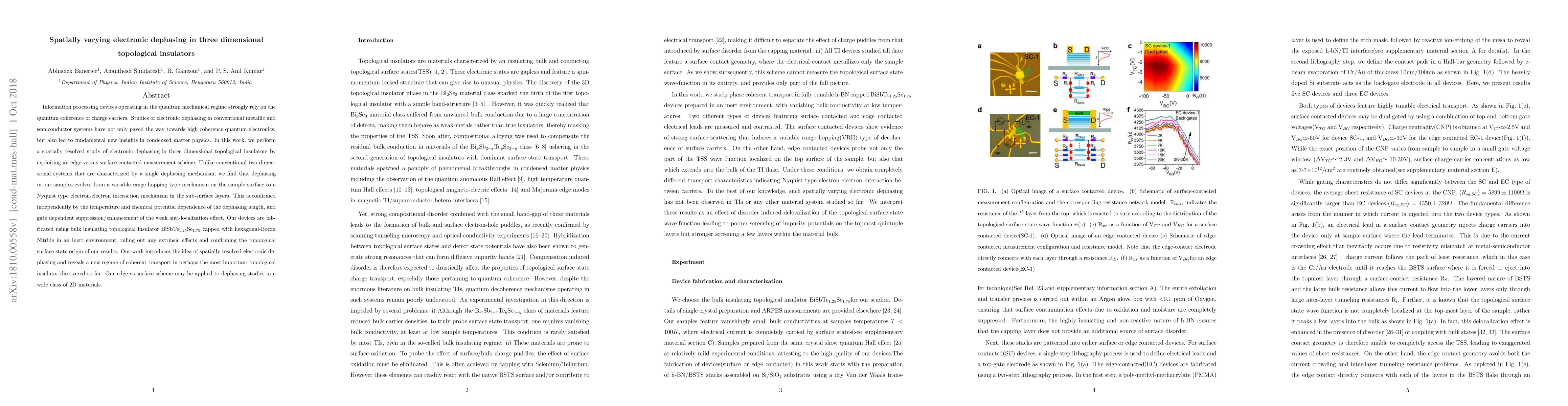
Spatially varying electronic dephasing in three dimensional topological insulators
Publication
Metrics
AI Quick Summary
This paper investigates spatially varying electronic dephasing in three-dimensional topological insulators using an edge versus surface contacted measurement scheme. The study reveals distinct dephasing mechanisms on the surface and sub-surface layers, suggesting a new regime of coherent transport in topological insulators.
Paper Preview
Abstract
Information processing devices operating in the quantum mechanical regime strongly rely on the quantum coherence of charge carriers. Studies of electronic dephasing in conventional metallic and semiconductor systems have not only paved the way towards high coherence quantum electronics, but also led to fundamental new insights in condensed matter physics. In this work, we perform a spatially resolved study of electronic dephasing in three dimensional topological insulators by exploiting an edge versus surface contacted measurement scheme. Unlike conventional two dimensional systems that are characterized by a single dephasing mechanism, we find that dephasing in our samples evolves from a variable-range-hopping type mechanism on the sample surface to a Nyquist type electron-electron interaction mechanism in the sub-surface layers. This is confirmed independently by the temperature and chemical potential dependence of the dephasing length, and gate dependent suppression/enhancement of the weak anti-localization effect. Our devices are fabricated using bulk insulating topological insulator BiSbTe$_{1.25}$Se$_{1.75}$ capped with hexagonal-Boron Nitride in an inert environment, ruling out any extrinsic effects and confirming the topological surface state origin of our results. Our work introduces the idea of spatially resolved electronic dephasing and reveals a new regime of coherent transport in perhaps the most important topological insulator discovered so far. Our edge-vs-surface scheme may be applied to dephasing studies in a wide class of 2D materials.
AI Key Findings
Get AI-generated insights about this paper's methodology, results, significance, and more — seven facets brought into focus.
Impact
Paper Details
PDF Preview
Key Terms
Citation Network
Current paper (gray), citations (green), references (blue)
Display is limited for performance on very large graphs.
Discussion 0