Summary
This work reports information on the transience of hole doping in epitaxial graphene devices when nitric acid is used as an adsorbent. Under vacuum conditions, desorption processes are monitored by electrical and spectroscopic means to extract the relevant timescales from the corresponding data. It is of vital importance to understand the reversible nature of hole doping because such device processing can be a suitable alternative to large-scale, metallic gating. Most measurements are performed post-exposure at room temperature, and, for some electrical transport measurements, at 1.5 K. Vacuum conditions are applied to many measurements to replicate the laboratory conditions under which devices using this doping method would be measured. The relevant timescales from transport measurements are compared with results from X-ray photoelecton spectroscopy and Fourier transform infrared spectroscopy measurements, with the latter performed at ambient conditions and accompanied by calculations of the spectra in the Reststrahlen band.
AI Key Findings
Get AI-generated insights about this paper's methodology, results, and significance.
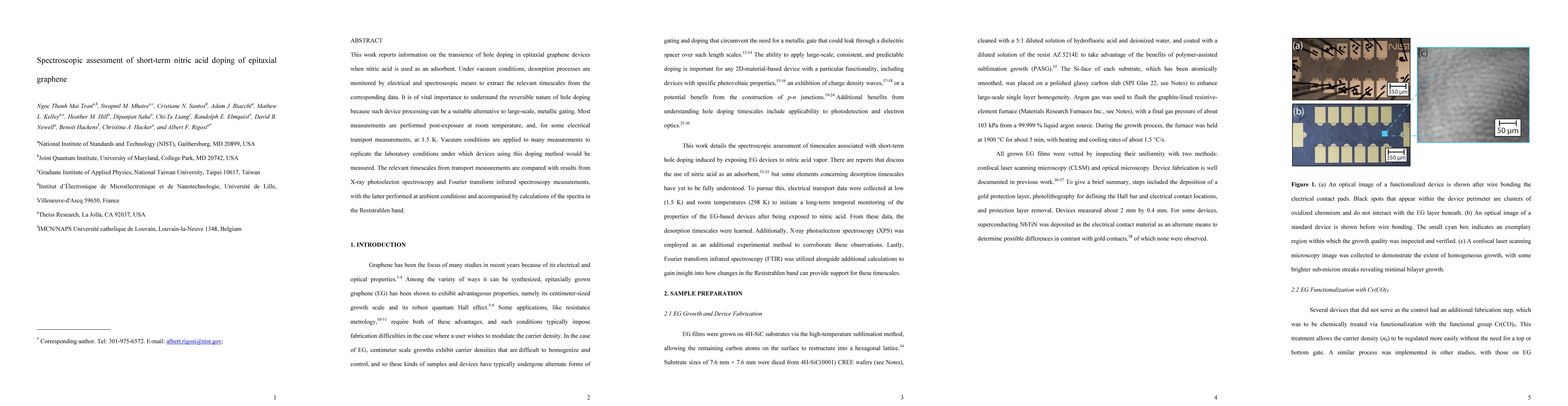
Paper Details
PDF Preview
Key Terms
Citation Network
Current paper (gray), citations (green), references (blue)
Display is limited for performance on very large graphs.
Similar Papers
Found 4 papersTimescales for Nitric Acid Desorption in Epitaxial Graphene Devices
Angela R. Hight Walker, Albert F. Rigosi, Ngoc Thanh Mai Tran et al.
No citations found for this paper.
Comments (0)