ArxivLens

Quick Summary:

This paper reviews spin and charge transport in graphene-based spin-valve devices with Co/MgO electrodes, highlighting two fabrication methods. The first method results in rough interfaces and conducting pinholes, with contact resistance being a key factor for spin dephasing. The second method, involving a graphene-hBN heterostructure, shows improved transport properties with high charge carrier mobilities and spin lifetimes, though analysis of spin scattering mechanisms is complicated.

Journal Reference: Synthetic Metals 210 Part A, 42 (2015)
DOI: 10.1016/j.synthmet.2015.07.007
arXiv Id: 1503.01735
Comments: 19 pages, 8 figures
Date Published: 2016-02-24
Date Updated: 2016-02-24

Categories:

Key Terms (TF-IDF):

mgo (0.293)
electrodes (0.241)
electrodes (0.239)
transport properties (0.233)
graphene (0.232)
graphene (0.227)
devices (0.218)
_c (0.206)
spin (0.205)
spin (0.203)
devices (0.201)
charge (0.190)
transport (0.185)
fabrication (0.185)
layer (0.185)
transport (0.183)
resistance (0.179)
charge (0.177)
layer (0.177)
resistance (0.171)
License: http://arxiv.org/licenses/nonexclusive-distrib/1.0/

Summary:

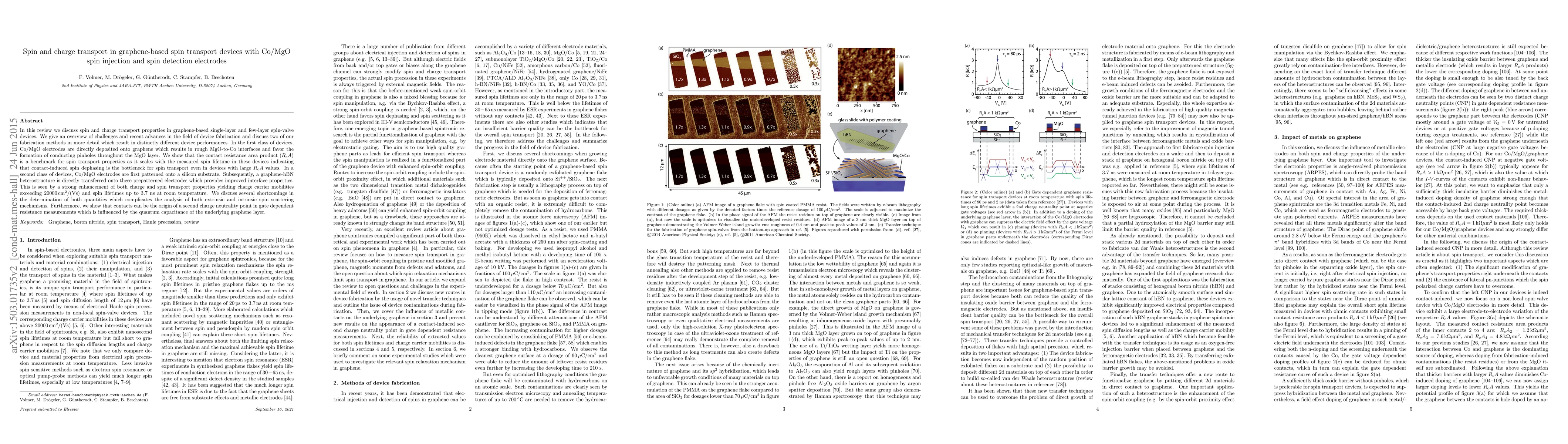
In this review we discuss spin and charge transport properties in graphene-based single-layer and few-layer spin-valve devices. We give an overview of challenges and recent advances in the field of device fabrication and discuss two of our fabrication methods in more detail which result in distinctly different device performances. In the first class of devices, Co/MgO electrodes are directly deposited onto graphene which results in rough MgO-to-Co interfaces and favor the formation of conducting pinholes throughout the MgO layer. We show that the contact resistance area product (R$_c$A) is a benchmark for spin transport properties as it scales with the measured spin lifetime in these devices indicating that contact-induced spin dephasing is the bottleneck for spin transport even in devices with large R$_c$A values. In a second class of devices, Co/MgO electrodes are first patterned onto a silicon substrate. Subsequently, a graphene-hBN heterostructure is directly transferred onto these prepatterned electrodes which provides improved interface properties. This is seen by a strong enhancement of both charge and spin transport properties yielding charge carrier mobilities exceeding 20000 cm$^2$/(Vs) and spin lifetimes up to 3.7 ns at room temperature. We discuss several shortcomings in the determination of both quantities which complicates the analysis of both extrinsic and intrinsic spin scattering mechanisms. Furthermore, we show that contacts can be the origin of a second charge neutrality point in gate dependent resistance measurements which is influenced by the quantum capacitance of the underlying graphene layer.

Citation & Reference Network Visualization

This graph shows how this paper is connected to other research. The current paper is shown in dark gray, papers that cite it are in green, and papers it references are in blue. You can:

Current Paper
Papers citing this work (Citations)
Papers cited by this work (References)

• Hover over any node to see the paper title

• Click a node to view that paper's details

• Drag nodes to rearrange the graph

• Use the zoom controls (bottom right) to zoom in/out

Citations and References

Title Authors Year Actions
Excitonic condensation and metal-semiconductor transition in AA bilayer graphene in an external magnetic field
V. Apinyan, T. Kopeć
2022
View Paper
Tunable Spin Injection in High-Quality Graphene with One-Dimensional Contacts
V. Guarochico-Moreira, J. Sambricio, K. Omari, Christopher R Anderson, D. Bandurin, J. Toscano-Figueroa, N. Natera-Cordero, Kenji Watanabe, T. Taniguchi, I. Grigorieva, I. J. Vera-Marun
2021
View Paper
Ultimate Spin Currents in Commercial Chemical Vapor Deposited Graphene
J. Panda, M. Ramu, O. Karis, T. Sarkar, M. Kamalakar
2020
View Paper
Spintronics in Two-Dimensional Materials
Yanping Liu, Cheng Zeng, Jiahong Zhong, Junnan Ding, Zhiming M. Wang, Zongwen Liu
2020
View Paper
Temperature dependence of static spin conductivity of gapped graphene
H. Rezania, R. Moradian, S. Marvi
2018
View Paper
Effect of Ti doping on spin injection and relaxation in few-layer graphene
Bing Zhao, Xiaoguang Xu, Le Wang, Juan Li, Ziyu Zhang, Pengfei Liu, Qi Liu, Zhicheng Wang, Yong Jiang
2018
View Paper
Measuring anisotropic spin relaxation in graphene
Sebastian Ringer, Stefan Hartl, Matthias Rosenauer, Tobias Volkl, Maximilian Kadur, Franz Hopperdietzel, D. Weiss, J. Eroms
2017
View Paper
Prospects of spintronics based on 2D materials
Y. Feng, Lei Shen, Ming Yang, Aizhu Wang, M. Zeng, Qingyun Wu, Sandhya Chintalapati, Ching‐Ray Chang
2017
View Paper
Electronic Spin Transport in Dual-Gated Bilayer Graphene
A. Avsar, I. J. Vera-Marun, J. Tan, G. Koon, Kenji Watanabe, T. Taniguchi, S. Adam, B. Ozyilmaz
2016
View Paper
Li-doped graphene for spintronic applications
N. Kheirabadi
2016
View Paper
Spin Lifetimes Exceeding 12 ns in Graphene Nonlocal Spin Valve Devices.
M. Drögeler, C. Franzen, F. Volmer, T. Pohlmann, L. Banszerus, M. Wolter, Kenji Watanabe, T. Taniguchi, C. Stampfer, B. Beschoten
2016
View Paper
Lithium doped graphene as spintronic devices
N. Kheirabadi
2015
View Paper
Nanosecond spin lifetimes in bottom‐up fabricated bilayer graphene spin‐valves with atomic layer deposited Al 2 O 3 spin injection and detection barriers
M. Drögeler, F. Volmer, M. Wolter, Kenji Watanabe, T. Taniguchi, D. Neumaier, C. Stampfer, B. Beschoten
2015
View Paper
Yanping Liu1,2,3 *, Cheng Zeng1, Jiahong Zhong1, Junnan Ding1, Zhiming M. Wang4 *, Zongwen Liu5 *
Yanping Liu, Cheng Zeng, Zhiming M. Wang, Zongwen Liu
2020
View Paper

Comments (0)

This website uses cookies to ensure you get the best experience. Learn more