Quick Summary:

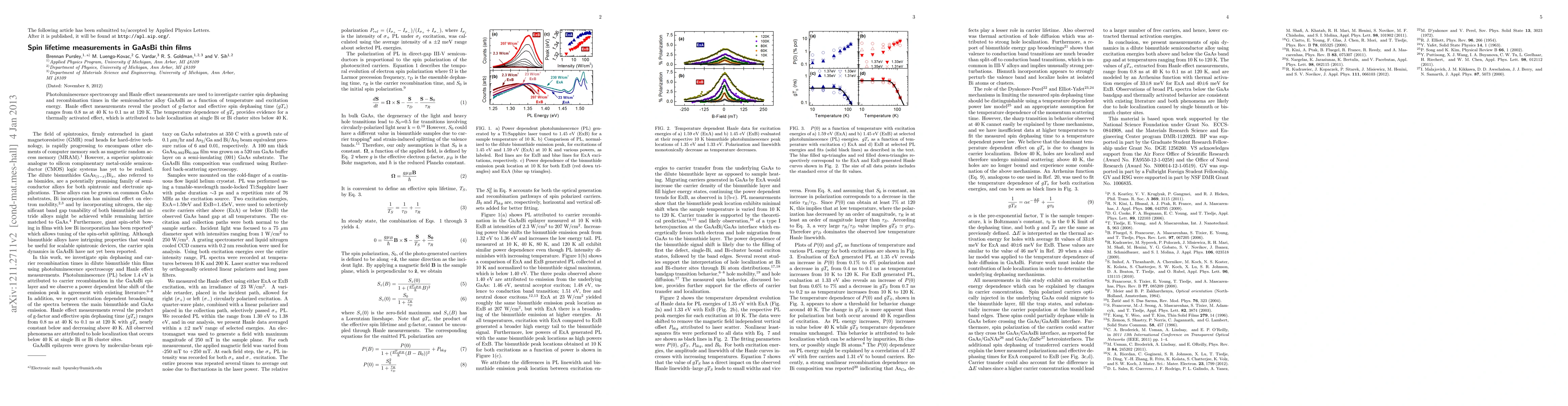
This study uses photoluminescence and Hanle effect measurements to analyze spin dephasing and recombination in GaAsBi thin films, finding that the g-factor times spin dephasing time (gTs) decreases from 0.8 ns at 40 K to 0.1 ns at 120 K, indicating a thermally activated effect due to hole localization at Bi sites.

Summary

Photoluminescence spectroscopy and Hanle effect measurements are used to investigate carrier spin dephasing and recombination times in the semiconductor alloy GaAsBi as a function of temperature and excitation energy. Hanle effect measurements reveal the product of g-factor and effective spin dephasing time (gTs) ranges from 0.8 ns at 40 K to 0.1 ns at 120 K. The temperature dependence of gTs provides evidence for a thermally activated effect, which is attributed to hole localization at single Bi or Bi cluster sites below 40 K.

AI Key Findings

Get AI-generated insights about this paper's methodology, results, and significance.

Paper Details

PDF Preview

Download PDF

Key Terms

dephasing (0.350)
ns (0.335)
ns (0.323)
bi (0.317)
bi (0.305)
effect (0.250)
effect (0.226)
recombination (0.218)
measurements (0.210)
spin (0.208)
attributed (0.204)
temperature dependence (0.200)
temperature (0.197)
semiconductor (0.193)
carrier (0.192)
spin (0.191)
measurements (0.190)
semiconductor (0.189)
recombination (0.189)
temperature (0.189)
Title Authors Year Actions
Temperature and band gap dependence of GaAsBi p-i-n diode current–voltage behaviour
R. Richards, F. Harun, M. M. Nawawi, Y. Liu, T. Rockett, J. David
2021
View Paper
Power loss mechanisms in n-type modulation-doped AlGaAs/GaAsBi quantum well heterostructures
O. Donmez, M. Aydın, S. Ardali, S. Yıldırım, E. Tiras, A. Erol, J. Puustinen, J. Hilska, M. Guina
2020
View Paper
Giant bowing of the band gap and spin-orbit splitting energy in GaP1−xBix dilute bismide alloys
Z. Bushell, C. Broderick, L. Nattermann, Rita Joseph, J. Keddie, J. Rorison, K. Volz, S. Sweeney
2019
View Paper
Raman spectroscopic determination of hole concentration in undoped GaAsBi
Sixin Zhu, W. Qiu, Han Wang, Tie Lin, Pingping Chen, Xingjun Wang
2018
View Paper
Conduction band electron relaxation and spin relaxation dynamics in CdZnTe alloy
L. Teng, Lijun Mu, Xia Wang
2018
View Paper
Bismuth content dependence of the electron spin relaxation time in GaAsBi epilayers and quantum well structures
S. Azaizia, A. Balocchi, S. Mazzucato, F. Cadiz, F. Beato de le Salle, H. Lehec, D. Lagarde, A. Arnoult, T. Amand, C. Fontaine, H. Carrère, X. Marie
2018
View Paper
Photovoltaic characterisation of GaAsBi/GaAs multiple quantum well devices
R. Richards, A. Mellor, F. Harun, J. S. Cheong, N. P. Hylton, T. Wilson, T. Thomas, J. Roberts, N. Ekins‐Daukes, J. David
2017
View Paper
Raman and AFM studies on nominally undoped, p- and n-type GaAsBi alloys
A. Erol, E. Akalin, K. Kara, M. Aslan, V. Bahrami-Yekta, R. Lewis, T. Tiedje
2017
View Paper
Indium-incorporation enhancement of photoluminescence properties of Ga(In)SbBi alloys
W. Linhart, M. Gładysiewicz, J. Kopaczek, M. Rajpalke, M. Ashwin, T. Veal, R. Kudrawiec
2017
View Paper
Optimisation of GaAsBi Based Semiconductors
Zhize Zhou
2017
View Paper
GaAs(1-x)Bix: A Promising Material for Optoelectronics Applications
K. K. Nagaraja, Y. Mityagin, M. P. Telenkov, I. Kazakov
2017
View Paper
Polarization resolved photoluminescence in GaAs1-xBix/GaAs quantum wells
M. Balanta, V. O. Gordo, A. Carvalho, J. Puustinen, H. Alghamdi, M. Henini, H. Galeti, M. Guina, Y. G. Gobato
2017
View Paper
Carrier dynamics in GaAsBi quantum wells
S. Azaizia, A. Balocchi, D. Lagarde, A. Arnoult, X. Marie, C. Fontaine, H. Carrère
2016
View Paper
Optical and spin properties of localized and free excitons in GaBixAs1−x/GaAs multiple quantum wells
M. Balanta, J. Kopaczek, V. Orsi Gordo, B. B. D. Santos, A. D. Rodrigues, H. Galeti, R. Richards, F. Bastiman, J. David, R. Kudrawiec, Y. Galvão Gobato
2016
View Paper
Deep level defects in dilute GaAsBi alloys grown under intense UV illumination
P. Mooney, M. Tarun, D. Beaton, A. Mascarenhas, K. Alberi
2016
View Paper
Anharmonicity in light scattering by optical phonons in GaAs1-xBix
R. S. Joshya, V. Rajaji, C. Narayana, A. Mascarenhas, R. Kini
2016
View Paper
Additional compound semiconductor nanowires for photonics
F. Ishikawa
2016
View Paper
Metamorphic GaAs/GaAsBi Heterostructured Nanowires.
F. Ishikawa, Yoshihiko Akamatsu, Kentaroh Watanabe, F. Uesugi, S. Asahina, U. Jahn, S. Shimomura
2015
View Paper
Composition dependent Raman intensity ratio between GaBi and GaAs mode in GaAsBi
W. Qiu, Xingjun Wang, Ning Li, Pingping Chen
2015
View Paper
Low- and high-energy photoluminescence from GaSb1−xBix with 0 < x ≤ 0.042
J. Kopaczek, R. Kudrawiec, W. Linhart, M. Rajpalke, T. Jones, M. Ashwin, T. Veal
2014
View Paper
Optical and Structural Properties of Emerging Dilute III-V Bismides
B. B. D. Santos, Y. G. Gobatoa, M. Heninib
2014
View Paper
Optical spin polarization and Hanle effect in GaAsSb: Temperature dependence
W. Qiu, Xingjun Wang, Pingping Chen, Ning-Sheng Li, W. Lu
2014
View Paper
Injection de spin dans des systèmes à base de semiconducteurs III-V en vue de nouveaux composants spintroniques
T. Zhang
2014
View Paper
Molecular beam epitaxy growth of GaAsBi using As2 and As4
R. Richards, F. Bastiman, C. Hunter, D. Mendes, A. Mohmad, J. Roberts, J. David
2014
View Paper
Magneto-optical properties of GaBiAs layers
A. Carvalho, V. O. Gordo, H. Galeti, Y. Galvão Gobato, M. D. de Godoy, R. Kudrawiec, O. M. Lemine, M. Henini
2014
View Paper
Temperature dependence of the band gap of GaSb1−xBix alloys with 0 < x ≤ 0.042 determined by photoreflectance
J. Kopaczek, R. Kudrawiec, W. Linhart, M. Rajpalke, K. Yu, T. Jones, M. Ashwin, J. Misiewicz, T. Veal
2013
View Paper
Electron spin dynamics and g-factor in GaAsBi
S. Mazzucato, T. Zhang, H. Carrère, D. Lagarde, P. Boonpeng, A. Arnoult, G. Lacoste, A. Balocchi, T. Amand, C. Fontaine, X. Marie
2013
View Paper
Investigation of Current Induced Spin Polarization in III-V Semiconductor Epilayers
M. Luengo-Kovac
2017
View Paper
Solar Energy Materials and Solar Cells Photovoltaic characterisation of GaAsBi/GaAs multiple quantum well devices
R. D. Richardsa, A. Mellorb, F. Haruna, J. S. Cheonga, N. P. Hyltonb, T. Wilsonb, T. Thomasb, J. S. Robertsa, N. J. Ekins-Daukesb, J. Davida
2017
View Paper

Comments (0)

This website uses cookies to ensure you get the best experience. Learn more