Spin-orbit interaction in three-dimensionally bounded semiconductor nanostructures
Publication
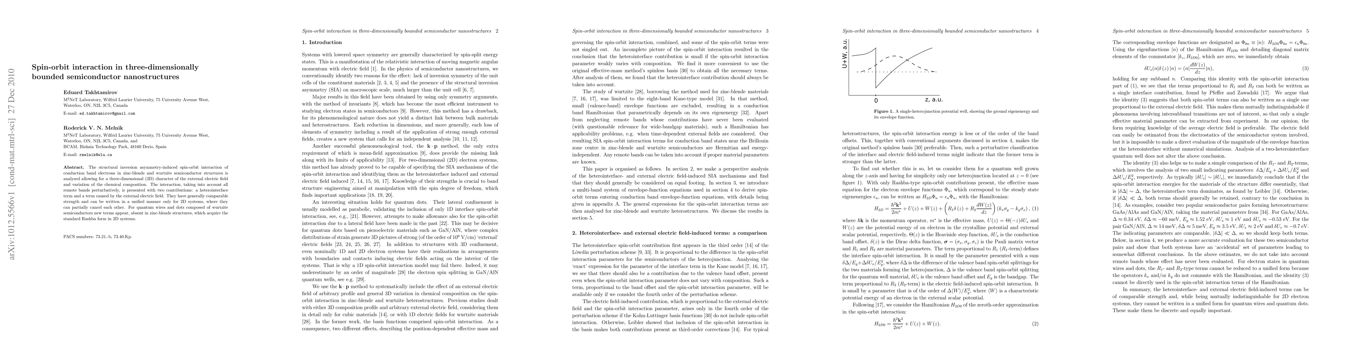
Metrics
AI Quick Summary
Researchers analyzed spin-orbit interaction in 3D semiconductor nanostructures, finding two contributions to this effect: a heterointerface term and an external electric field term that cancel each other in 2D systems but have comparable strength in 3D structures.
Paper Preview
Abstract
The structural inversion asymmetry-induced spin-orbit interaction of conduction band electrons in zinc-blende and wurtzite semiconductor structures is analysed allowing for a three-dimensional (3D) character of the external electric field and variation of the chemical composition. The interaction, taking into account all remote bands perturbatively, is presented with two contributions: a heterointerface term and a term caused by the external electric field. They have generally comparable strength and can be written in a unified manner only for 2D systems, where they can partially cancel each other. For quantum wires and dots composed of wurtzite semiconductors new terms appear, absent in zinc-blende structures, which acquire the standard Rashba form in 2D systems.
AI Key Findings
Get AI-generated insights about this paper's methodology, results, significance, and more — seven facets brought into focus.
Impact
Paper Details
PDF Preview
Key Terms
Citation Network
Current paper (gray), citations (green), references (blue)
Display is limited for performance on very large graphs.
Discussion 0