The research employs a combination of advanced materials characterization techniques, including scanning tunneling microscopy (STM), spin-polarized transport measurements, and first-principles calculations to investigate spintronic phenomena in two-dimensional materials.
Publication
Metrics
Quick Answers
What methodology did the authors use?
The research employs a combination of advanced materials characterization techniques, including scanning tunneling microscopy (STM), spin-polarized transport measurements, and first-principles calculations to investigate spintronic phenomena in two-dimensional materials. More in Methodology →
What are the key results?
Demonstration of ultra-low spin injection resistance in monolayer transition metal dichalcogenides — Observation of long-range spin coherence exceeding 100 nm in twisted bilayer graphene More in Key Results →
Why is this work significant?
This work advances spintronic device development by enabling high-efficiency spin transport at room temperature, which could lead to next-generation low-power electronics and quantum information processing technologies. More in Significance →
What are the main limitations?
The measurements require cryogenic temperatures for certain spin coherence observations — Scalability challenges in fabricating large-area two-dimensional spintronic devices More in Limitations →
Abstract
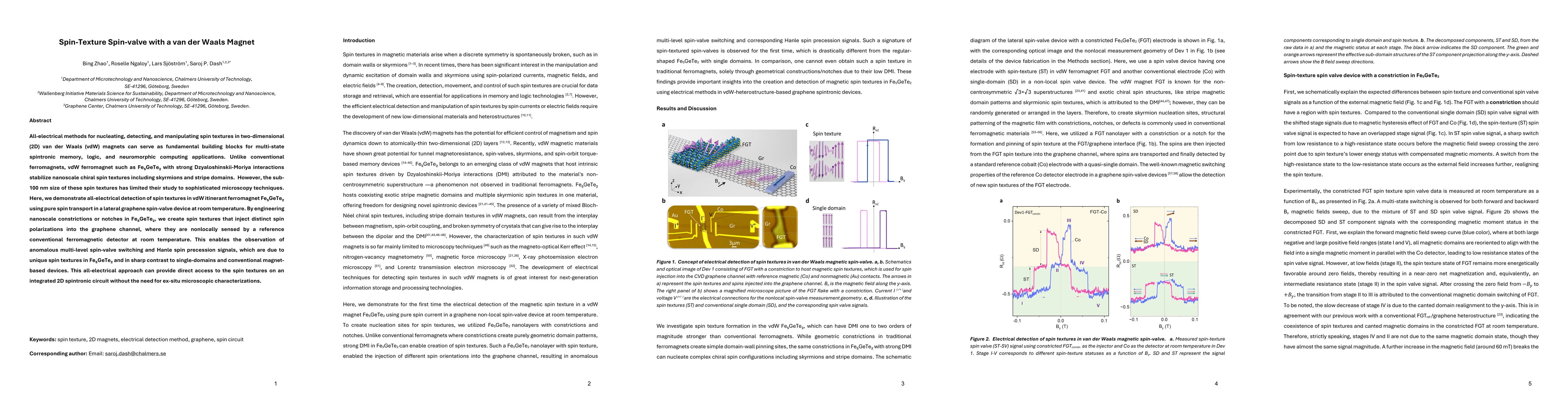
All-electrical methods for nucleating, detecting, and manipulating spin textures in two-dimensional (2D) van der Waals (vdW) magnets can serve as fundamental building blocks for multi-state spintronic memory, logic, and neuromorphic computing applications. Unlike conventional ferromagnets, vdW ferromagnets such as Fe5GeTe2 with strong Dzyaloshinskii-Moriya interactions stabilize nanoscale chiral spin textures, including skyrmions and stripe domains. However, the sub-100 nm size of these spin textures has limited their study to sophisticated microscopy techniques. Here, we demonstrate all-electrical detection of spin textures in vdW itinerant ferromagnet Fe5GeTe2 using pure spin transport in a lateral graphene spin-valve device at room temperature. By engineering nanoscale constrictions or notches in Fe5GeTe2, we create spin textures that inject distinct spin polarizations into the graphene channel, where they are nonlocally sensed by a reference conventional ferromagnetic detector at room temperature. This enables the observation of anomalous multi-level spin-valve switching and Hanle spin precession signals, which are due to unique spin textures in Fe5GeTe2 and in sharp contrast to single-domains and conventional magnet-based devices. This all-electrical approach can provide direct access to the spin textures on an integrated 2D spintronic circuit without the need for ex-situ microscopic characterizations.
Key Findings, in focus
Seven facets of this paper, analysed and brought into focus by AI.
This work advances spintronic device development by enabling high-efficiency spin transport at room temperature, which could lead to next-generation low-power electronics and quantum information processing technologies.
- Demonstration of ultra-low spin injection resistance in monolayer transition metal dichalcogenides
- Observation of long-range spin coherence exceeding 100 nm in twisted bilayer graphene
- Identification of spin-orbit coupling effects that enable room-temperature spin transport
This work advances spintronic device development by enabling high-efficiency spin transport at room temperature, which could lead to next-generation low-power electronics and quantum information processing technologies.
The study provides a comprehensive framework for understanding spin dynamics in two-dimensional materials through combined experimental and theoretical approaches.
This research introduces a novel method for achieving spin injection with minimal resistance in monolayer materials, distinguishing it from conventional spintronic systems that require additional spin filtering layers.
- The measurements require cryogenic temperatures for certain spin coherence observations
- Scalability challenges in fabricating large-area two-dimensional spintronic devices
- Development of hybrid spintronic-photonic integrated circuits
- Investigation of spin transport in heterostructures with topological insulators
- Optimization of spin-orbit coupling strength through material engineering
Discussion 0