Publication
Metrics
AI Quick Summary
Sputtering is gaining attention for growing large-area TMDC materials for solid-state device applications, such as FETs and photodetectors.
Paper Preview
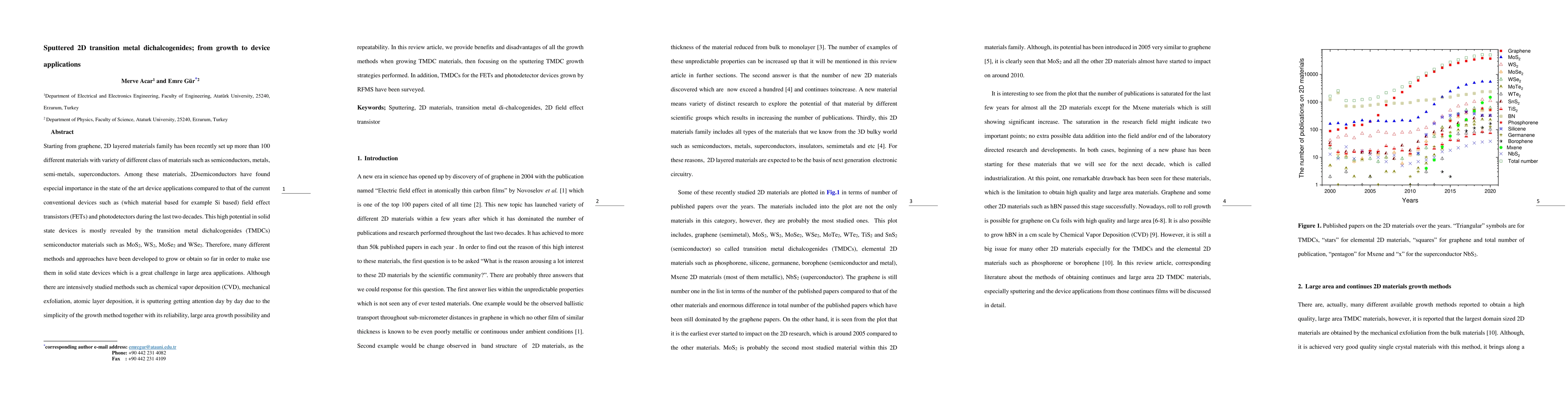
Abstract
Starting from graphene, 2D layered materials family has been recently set up more than 100 different materials with variety of different class of materials such as semiconductors, metals, semimetals, superconductors. Among these materials, 2D semiconductors have found especial importance in the state of the art device applications compared to that of the current conventional devices such as (which material based for example Si based) field effect transistors (FETs) and photodetectors during the last two decades. This high potential in solid state devices is mostly revealed by the transition metal dichalcogenides (TMDCs) semiconductor materials such as MoS2 , WS2 , MoSe2 and WSe2 . Therefore, many different methods and approaches have been developed to grow or obtain so far in order to make use them in solid state devices, which is a great challenge in large area applications. Although there are intensively studied methods such as chemical vapor deposition (CVD), mechanical exfoliation, atomic layer deposition, it is sputtering getting attention day by day due to the simplicity of the growth method together with its reliability, large area growth possibility and repeatability. In this review article, we provide benefits and disadvantages of all the growth methods when growing TMDC materials, then focusing on the sputtering TMDC growth strategies performed. In addition, TMDCs for the FETs and photodetector devices grown by RFMS have been surveyed.
AI Key Findings
Get AI-generated insights about this paper's methodology, results, significance, and more — seven facets brought into focus.
Impact
Paper Details
Authors
PDF Preview
Key Terms
Citation Network
Current paper (gray), citations (green), references (blue)
Display is limited for performance on very large graphs.
Discussion 0