Stacked Wafer Gradient Index Silicon Optics with Integral Anti-reflection Layers

Source: ArXiv

AI Quick Summary

This paper develops silicon optics with wide bandwidth anti-reflection coatings for millimeter and submillimeter wavelengths, utilizing multi-layer textured surfaces and DRIE fabrication. Experimental results on high resistivity silicon wafers show optimal transmission around 250 GHz, validated by simulations.

Share: Share on X LinkedIn

Summary

Silicon optics with wide bandwidth anti-reflection (AR) coatings, made of multi-layer textured silicon surfaces, are developed for millimeter and submillimeter wavelengths. Single and double layer AR coatings were designed for an optimal transmission centered on 250 GHz, and fabricated using the DRIE (Deep Reaction Ion Etching) technique. Tests of high resistivity silicon wafers with single-layer coatings between 75 GHz and 330 GHz are presented and compared with the simulations.

AI Key Findings

Generated Sep 03, 2025

Methodology

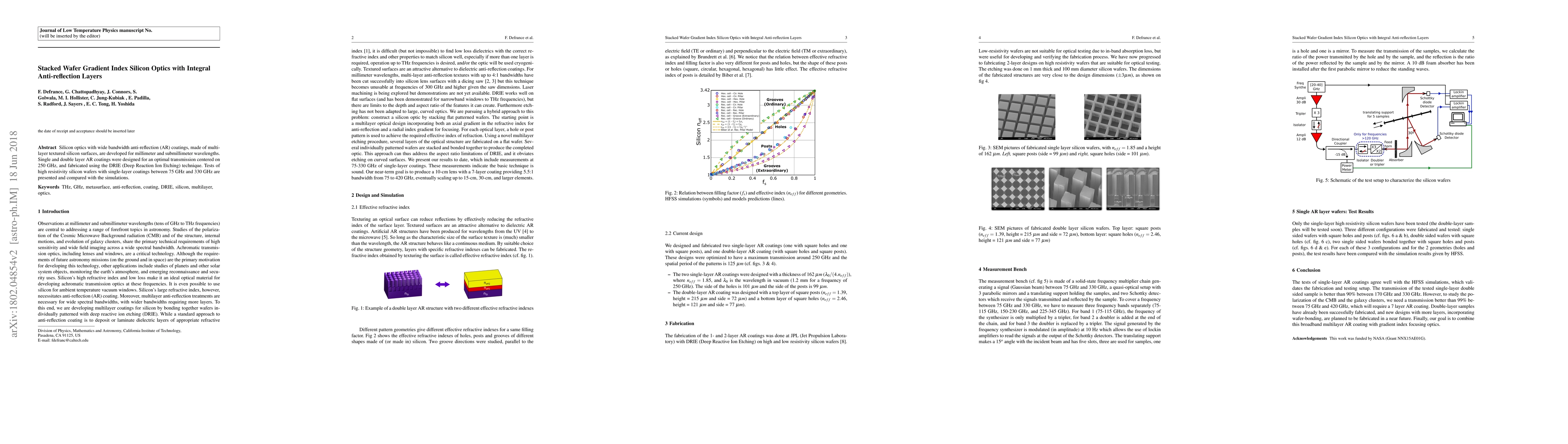
The research utilized Deep Reactive Ion Etching (DRIE) to fabricate single and double layer anti-reflection (AR) coatings on high and low resistivity silicon wafers. The designs were optimized for maximum transmission around 250 GHz with a spatial period of 125 µm. Measurements were conducted using a solid-state frequency multiplier chain and a quasi-optical setup with parabolic mirrors and Schottky detectors, covering frequency bands from 75 GHz to 330 GHz.

Key Results

  • Single-layer high-resistivity silicon wafers with square holes and posts, as well as double-sided square hole wafers, showed good agreement with HFSS simulations, validating the fabrication and testing setup.
  • The transmission of a tested single-layer double-sided sample exceeded 90% between 170 GHz and 330 GHz.
  • To meet the requirements for studying CMB and galaxy clusters, a 7-layer AR coating with transmission better than 99% between 75 GHz and 420 GHz is planned.

Significance

This research is significant for developing low-loss dielectrics with appropriate refractive indices for silicon optics, especially for use in cryogenic conditions and up to THz frequencies. The hybrid approach of stacking flat patterned wafers addresses the limitations of DRIE in terms of depth and spectral range of features, and avoids etching on curved surfaces.

Technical Contribution

The paper presents a novel method for creating stacked wafer gradient index silicon optics with integral anti-reflection layers, utilizing a hybrid approach of flat patterned wafer stacking to overcome DRIE limitations.

Novelty

This work introduces a new technique for creating silicon optics with wide bandwidth anti-reflection coatings using multi-layer textured silicon surfaces, which is particularly advantageous for millimeter and submillimeter wavelengths.

Limitations

  • The current study only tested single-layer AR coatings; double-layer samples are yet to be tested.
  • The fabricated structures are limited to flat surfaces, and the approach has not yet been demonstrated for large, curved optics.

Future Work

  • Plan to produce a 10 cm lens with a 7-layer coating providing 5.5:1 bandwidth from 75 to 420 GHz.
  • Scale up to larger elements like 15 cm, 30 cm, and beyond.

Paper Details

PDF Preview

Download PDF

Key Terms

silicon (0.367)
ghz (0.348)
ar (0.322)
layer (0.274)
resistivity (0.187)
centered (0.187)
millimeter (0.186)
wavelengths (0.177)

Citation Network

Current paper (gray), citations (green), references (blue)

Display is limited for performance on very large graphs.

Current Paper
Citations
References
Click to view

No citations found for this paper.

Comments (0)

This website uses cookies to ensure you get the best experience. Learn more