Strain effect engineered in {\alpha}-Al2O3/monolayer MoS2 interface by first principle calculations
Publication
Metrics
AI Quick Summary
This study uses first principle calculations to investigate the strain effect at the interface between Al2O3 and monolayer MoS2, revealing that a 1.3nm thick Al2O3 layer induces a 0.3% strain on MoS2. The research suggests that dielectric engineering can effectively manipulate strain in nanotechnological applications.
Paper Preview
Abstract
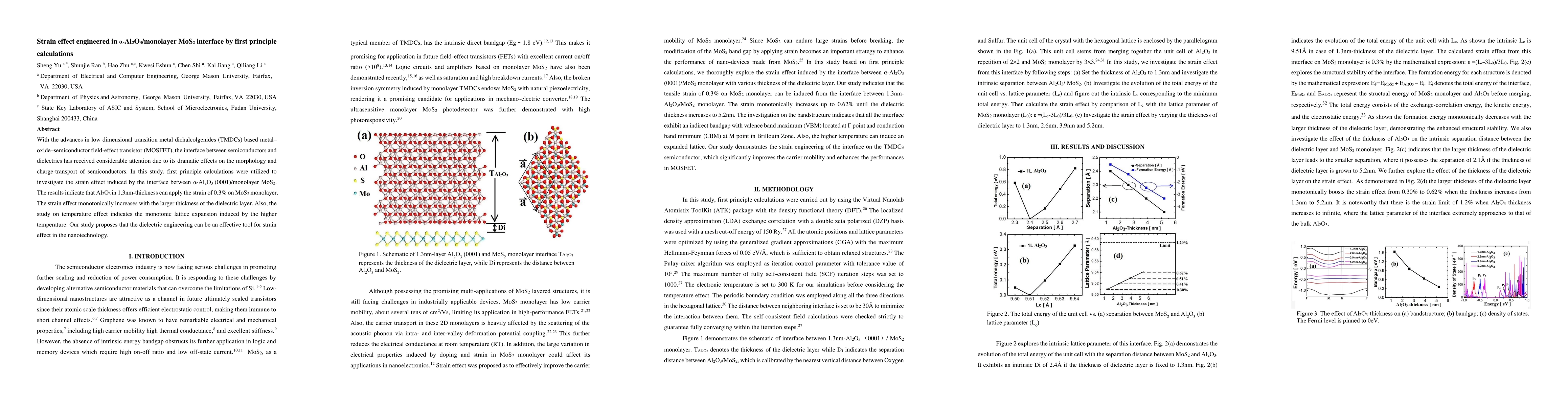
With the advances in low dimensional transition metal dichalcolgenides (TMDCs) based metal oxide semiconductor field effect transistor (MOSFET), the interface between semiconductors and dielectrics has received considerable attention due to its dramatic effects on the morphology and charge transport of semiconductors. In this study, first principle calculations were utilized to investigate the strain effect induced by the interface between Al2O3 (0001) and monolayer MoS2. The results indicate that Al2O3 in 1.3nm thickness can apply the strain of 0.3% on MoS2 monolayer. The strain effect monotonically increases with the larger thickness of the dielectric layer. Also, the study on temperature effect indicates the monotonic lattice expansion induced by the higher temperature. Our study proposes that the dielectric engineering can be an effective tool for strain effect in the nanotechnology.
AI Key Findings
Get AI-generated insights about this paper's methodology, results, significance, and more — seven facets brought into focus.
Paper Details
PDF Preview
Key Terms
Related Papers
No references found for this paper.
Discussion 0