ArxivLens

Quick Summary:

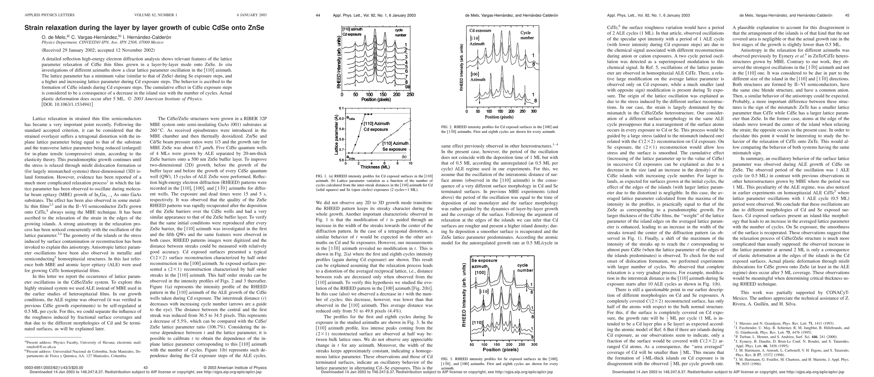
This study uses reflection high-energy electron diffraction to analyze the lattice parameter relaxation during layer-by-layer growth of cubic CdSe on ZnSe, revealing oscillations in the 110 azimuth. The observed lattice parameter minimum during Se exposure and increase during Cd exposure suggest the formation of CdSe islands, with plastic deformation occurring after five monolayers.

Journal Reference: Appl. Phys. Lett. 82, 2003, 43
DOI: 10.1063/1.1534941
arXiv Id: 1910.02943
Date Published: 2019-10-09
Date Updated: 2019-10-09

Categories:

Key Terms (TF-IDF):

exposure (0.376)
steps (0.305)
cd (0.292)
lattice (0.241)
parameter (0.212)
layer (0.183)
situ (0.166)
cumulative (0.159)
analysis shows (0.149)
diffraction (0.146)
investigations (0.144)
ml (0.143)
cycles (0.143)
reflection (0.139)
films (0.139)
actual (0.139)
oscillation (0.134)
decrease (0.132)
deformation (0.130)
high energy (0.129)
License: http://arxiv.org/licenses/nonexclusive-distrib/1.0/

Summary:

A detailed reflection high-energy electron diffraction analysis shows relevant features of the lattice parameter relaxation of CdSe thin films grown in a layer-by-layer mode onto ZnSe. In situ investigations of different azimuths show a clear lattice parameter oscillation in the 110 azimuth. The lattice parameter has a minimum value ~similar to that of ZnSe! during Se exposure steps, and a higher and increasing lattice parameter during Cd exposure steps. The behavior is ascribed to the formation of CdSe islands during Cd exposure steps. The cumulative effect in CdSe exposure steps is considered to be a consequence of a decrease in the island size with the number of cycles. Actual plastic deformation does occur after 5 ML.

Citation & Reference Network Visualization

This graph shows how this paper is connected to other research. The current paper is shown in dark gray, papers that cite it are in green, and papers it references are in blue. You can:

Current Paper
Papers citing this work (Citations)
Papers cited by this work (References)

• Hover over any node to see the paper title

• Click a node to view that paper's details

• Drag nodes to rearrange the graph

• Use the zoom controls (bottom right) to zoom in/out

Citations and References

Title Authors Year Actions
Strain Effects in Epitaxial VO2 Thin Films on Columnar Buffer-Layer TiO2/Al2O3 Virtual Substrates.
E. Breckenfeld, Heungsoo Kim, K. Burgess, N. Charipar, S. Cheng, R. Stroud, A. Piqué
2017
View Paper
Stress effects on the photoluminescence energies and binding energies of excitons in ultra-thin ZnTe/CdTe/ZnTe quantum wells
M. F. Vargas-Charry, C. Vargas-Hernández
2016
View Paper
Study of the coupling of ultra-thin CdSe double quantum wells
J. A. Lorenzo-Andrade, František Šutara, I. Hernández-Calderón
2015
View Paper
Structures de semiconducteurs II-VI à alignement de bandes de type II pour le photovoltaïque
L. Gérard
2013
View Paper
Strain evolution in non-stoichiometric heteroepitaxial thin-film perovskites
E. Breckenfeld, A. Shah, L. Martin
2013
View Paper
Vapour transport and inner walls covering in large aspect ratio macropores
O. Melo, S. Larramendi, M. Hernández-Vélez
2012
View Paper
Infrared reflectance and transmission spectra in II-VI alloys and superlattices
D. Talwar, Tzuen-Rong Yang, Z. Feng, P. Becla
2011
View Paper
On the isothermal closed space sublimation growth of CdSe using a mixed source for selenium
E. M. Larramendi, Z-B Karla Gutiérrez, O. Melo, U. Woggon, D. Schikora, K. Lischka
2010
View Paper
Determination of critical thickness for defect formation of CdSe/ZnSe heterostructures by transmission electron microscopy and photoluminescence spectroscopy
D. Litvinov, M. Schowalter, A. Rosenauer, B. Daniel, J. Fallert, W. Löffler, H. Kalt, M. Hetterich
2008
View Paper
CdSe quantum dot formation: alternative paths to relaxation of a strained CdSe layer and influence of the capping conditions
I. Robin, T. Aichele, C. Bougerol, R. André, S. Tatarenko, E. Bellet-Amalric, B. van Daele, G. van Tendeloo
2007
View Paper
Elastic and surface energies: Two key parameters for CdSe quantum dot formation
I. Robin, R. André, C. Bougerol, T. Aichele, S. Tatarenko
2006
View Paper
Growth modes transition induced by strain relaxation in epitaxial MgO thin films on SrTiO3 (001) substrates
Yu Li, Z. Liang, Ying Zhang, Jinfeng Zhu, Shuwen Jiang, Xianhua Wei
2005
View Paper
Control of the two-dimensional–three-dimensional transition of self-organized CdSe/ZnSe quantum dots
I. Robin, R. André, H. Mariette, S. Tatarenko, L. S. Dang, Joël Bleuse, E. Bellet-Amalric, J. Gerard
2005
View Paper
Molecular beam epitaxial growth and characterization of Cd-based II–VI wide-bandgap compounds on Si substrates
G. Brill, Y. Chen, P. M. Amirtharaj, W. Sarney, D. Chandler-Horowitz, N. Dhar
2005
View Paper
New method to induce 2D–3D transition of strained CdSe/ZnSe layers
I. Robin, R. André, H. Mariette, S. Tatarenko, L. S. Dang, J. Gerard, E. Bellet-Amalric
2005
View Paper
Growth and characterization of ultra‐thin quantum wells of II–VI semiconductors for optoelectronic applications
I. Hernández-Calderón, M. García-Rocha, P. Dı́az-Arencibia
2004
View Paper
Mechanical properties and band structure of CdSe and CdTe nanostructures at high pressure - a first-principles study
N. Kishore, V. Nagarajan, R. Chandiramouli
2019
View Paper
7.4.2 CdSe/ZnSe quantum dots
F. Henneberger
2013
View Paper
Epitaxial growth of thin films and quantum structures of II–VI visible-bandgap semiconductors
I. Hernández-Calderón
2013
View Paper

Comments (0)

This website uses cookies to ensure you get the best experience. Learn more