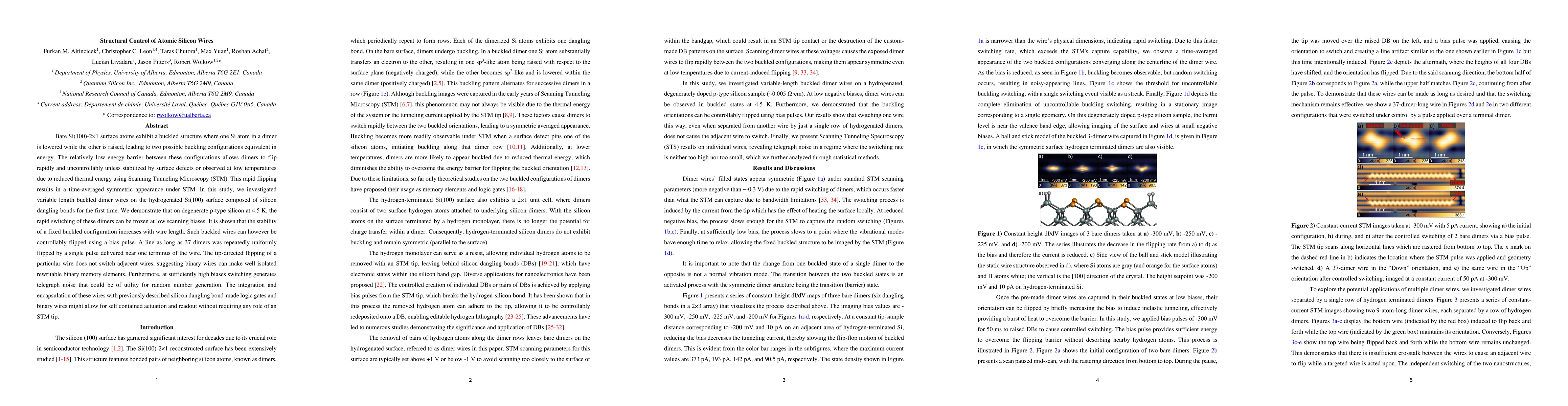
Electronic structures of atomic silicon dimer wires as a function of length
|
Furkan Altincicek, L. Livadaru, Christopher C. Leon, Taras Chutora, Max Yuan, R. Achal, Jeremiah Croshaw, J. Pitters, R. Wolkow
|
2024
|
View Paper
|
Atomically Precise Manufacturing of Silicon Electronics
|
J. Pitters, Jeremiah Croshaw, R. Achal, L. Livadaru, S. Ng, Robert Lupoiu, Taras Chutora, Taleana R Huff, Konrad Walus, R. Wolkow
|
2024
|
View Paper
|
The Need for Speed: Efficient Exact Simulation of Silicon Dangling Bond Logic
|
Jan Drewniok, Marcel Walter, Robert Wille
|
2023
|
View Paper
|
QuickSim: Efficient and Accurate Physical Simulation of Silicon Dangling Bond Logic
|
Jan Drewniok, Marcel Walter, Samuel Sze Hang Ng, K. Waluś, R. Wille
|
2023
|
View Paper
|
Enhanced Atomic Precision Fabrication by Adsorption of Phosphine into Engineered Dangling Bonds on H-Si Using STM and DFT.
|
Jonathan Wyrick, Xiqiao Wang, Pradeep Namboodiri, R. Kashid, Fan Fei, Joseph Fox, R. Silver
|
2021
|
View Paper
|
Atom-by-Atom Construction of a Cyclic Artificial Molecule in Silicon.
|
Jonathan Wyrick, Xiqiao Wang, Pradeep Namboodiri, S. Schmucker, R. Kashid, R. Silver
|
2018
|
View Paper
|
SiQAD: A Design and Simulation Tool for Atomic Silicon Quantum Dot Circuits
|
S. Ng, R. Wolkow, K. Waluś, Jacob Retallick, H. N. Chiu, Robert Lupoiu, L. Livadaru, Taleana R Huff, M. Rashidi, Wyatt Vine, T. Dienel
|
2018
|
View Paper
|
Lithography for robust and editable atomic-scale silicon devices and memories
|
R. Achal, M. Rashidi, Jeremiah Croshaw, D. Churchill, M. Taucer, Taleana R Huff, Martin Cloutier, J. Pitters, R. Wolkow
|
2018
|
View Paper
|
Tip-induced passivation of dangling bonds on hydrogenated Si(100)-2 × 1
|
N. Pavliček, Z. Majzik, G. Meyer, L. Gross
|
2017
|
View Paper
|
Binary atomic silicon logic
|
Taleana R Huff, H. Labidi, M. Rashidi, L. Livadaru, T. Dienel, R. Achal, Wyatt Vine, J. Pitters, R. Wolkow
|
2017
|
View Paper
|
Atomic White-Out: Enabling Atomic Circuitry through Mechanically Induced Bonding of Single Hydrogen Atoms to a Silicon Surface.
|
Taleana R Huff, H. Labidi, M. Rashidi, M. Koleini, R. Achal, M. Salomons, R. Wolkow
|
2017
|
View Paper
|
The butterfly - a well-defined constant-current topography pattern on Si(001):H and Ge(001):H resulting from current-induced defect fluctuations.
|
M. Engelund, S. Godlewski, M. Kolmer, Rafal Zuzak, B. Such, T. Frederiksen, M. Szymoński, D. Sánchez-Portal
|
2016
|
View Paper
|
Origin of Symmetric Dimer Images of Si(001) Observed by Low-Temperature Scanning Tunneling Microscopy
|
Xiaoyan Ren, Hyunjung Kim, C. Niu, Yu Jia, Jun-Hyung Cho
|
2015
|
View Paper
|
Atomic scale study of corrugating and anticorrugating states on the bare Si(1 0 0) surface
|
M. Yengui, H. Pinto, J. Leszczynski, D. Riedel
|
2015
|
View Paper
|
Silicon Atomic Quantum Dots Enable Beyond-CMOS Electronics
|
R. Wolkow, L. Livadaru, J. Pitters, M. Taucer, P. Piva, M. Salomons, Martin Cloutier, B. V. C. Martins
|
2013
|
View Paper
|
Engineering the electronic structure of surface dangling bond nanowires of different size and dimensionality
|
B. Naydenov, J. Boland
|
2013
|
View Paper
|
Quantum engineering at the silicon surface using dangling bonds
|
S. R. Schofield, S. R. Schofield, P. Studer, P. Studer, C. Hirjibehedin, C. Hirjibehedin, N. Curson, N. Curson, G. Aeppli, G. Aeppli, D. Bowler, D. Bowler
|
2013
|
View Paper
|
Gwyddion: an open-source software for SPM data analysis
|
D. Nečas, P. Klapetek
|
2012
|
View Paper
|
Manipulating Si(100) at 5 K using qPlus frequency modulated atomic force microscopy: Role of defects and dynamics in the mechanical switching of atoms
|
A. Sweetman, S. Jarvis, R. Danza, J. Bamidele, L. Kantorovich, P. Moriarty
|
2011
|
View Paper
|
Tungsten nanotip fabrication by spatially controlled field-assisted reaction with nitrogen.
|
M. Rezeq, J. Pitters, R. Wolkow
|
2006
|
View Paper
|
STM excitation of individual biphenyl molecules on Si(1 0 0) surface: DIET or DIEF?
|
M. Cranney, A. Mayne, A. Laikhtman, G. Comtet, G. Dujardin
|
2005
|
View Paper
|
Influence of tip-surface interactions and surface defects on Si(100) surface structures by low-temperature (5 K) scanning tunneling microscopy
|
D. Riedel, M. Lastapis, M. Martin, G. Dujardin
|
2004
|
View Paper
|
Vibration of the dimer on Si(001) surface excited by STM current
|
H. Kawai, O. Narikiyo
|
2003
|
View Paper
|
Dimer buckling of the Si(001)2×1 surface below 10 K observed by low-temperature scanning tunneling microscopy
|
M. Ono, A. Kamoshida, N. Matsuura, E. Ishikawa, T. Eguchi, Y. Hasegawa
|
2003
|
View Paper
|
Alternative paradigm for physical computing.
|
I. Appelbaum, J. Joannopoulos, V. Narayanamurti
|
2002
|
View Paper
|
Can silicon dimers form logic gates
|
I. Appelbaum, Tairan Wang, S. Fan, J. Joannopoulos, V. Narayanamurti
|
2001
|
View Paper
|
Atomically resolved local variation of the barrier height of the flip-flop motion of single buckled dimers of Si(100).
|
K. Hata, Y. Sainoo, H. Shigekawa
|
2001
|
View Paper
|
Dynamic force microscopy of copper surfaces : atomic resolution and distance dependence of tip-sample interaction and tunneling current
|
C. Loppacher, M. Bammerlin, M. Guggisberg, S. Schär, R. Bennewitz, A. Baratoff, E. Meyer, H. Güntherodt
|
2000
|
View Paper
|
Novel methods for preparing EC STM tips
|
R. Kazinczi, E. Szőcs, E. Kálmán, P. Nagy
|
1998
|
View Paper
|
Dangling bond dynamics on the silicon (100)-2x1 surface: dissociation, diffusion, and recombination
|
McEllistrem, Allgeier, Boland
|
1998
|
View Paper
|
Nanoscale patterning and selective chemistry of silicon surfaces by ultrahigh-vacuum scanning tunneling microscopy
|
J. Lyding, T. Shen, G. Abeln, C. Wang, J. Tucker
|
1996
|
View Paper
|
Flipping silicon dimers on Si(100) using scanning tip microscopy: A theoretical investigation.
|
Cho, Joannopoulos
|
1996
|
View Paper
|
Atomic-Scale Desorption Through Electronic and Vibrational Excitation Mechanisms
|
T. Shen, C. Wang, G. Abeln, J. Tucker, J. Lyding, P. Avouris, R. Walkup
|
1995
|
View Paper
|
Theoretical study of the Si(100) surface reconstruction.
|
A. Ramstad, G. Brocks, Paul J. Kelly
|
1995
|
View Paper
|
Direct observation of an increase in buckled dimers on Si(001) at low temperature.
|
R. Wolkow
|
1992
|
View Paper
|
Site-dependent electronic effects, forces, and deformations in scanning tunneling microscopy of flat metal surfaces.
|
Ciraci, Baratoff, Batra
|
1990
|
View Paper
|
Scanning tunneling microscopy of Si(001).
|
R. J. Hamers, R. Tromp, J. Demuth
|
1986
|
View Paper
|
Si(001) Dimer structure observed with scanning tunneling microscopy.
|
Tromp, Hamers, Demuth
|
1985
|
View Paper
|
Atomic and Electronic Structures of Reconstructed Si(100) Surfaces
|
D. Chadi
|
1979
|
View Paper
|
The Si (100) surface. III. Surface reconstruction
|
J. Appelbaum, G. Baraff, D. Hamann
|
1976
|
View Paper
|
Structure and Adsorption Characteristics of Clean Surfaces of Germanium and Silicon
|
R. Schlier, H. E. Farnsworth
|
1959
|
View Paper
|
DIET at the nanoscale
|
G. Dujardin, E. Boer-Duchemin, E. Moal, A. Mayne, D. Riedel
|
2016
|
View Paper
|
chains fabricated on a Hydrogen-Terminated SI(100)-2×1 Surface
|
|
1999
|
|
Cluster study of the Si(111)2×1 reconstruction
|
P. Badziag, W. Verwoerd
|
1988
|
View Paper
|
Jahn-Teller distortion in Dangling-Bond linear
|
|
|
|
Comments (0)