Structure and electrical behavior of silicon nanowires prepared by MACE process
Publication
Metrics
AI Quick Summary
This paper investigates the structure and electrical behavior of silicon nanowire arrays prepared via MACE, revealing merged parallel nanowires with lengths of 700 nm and 1000 nm. The study shows memristive I-V characteristics attributed to trap states, with photoluminescence and transient spectroscopy indicating higher defect density in longer wires.
Paper Preview
Abstract
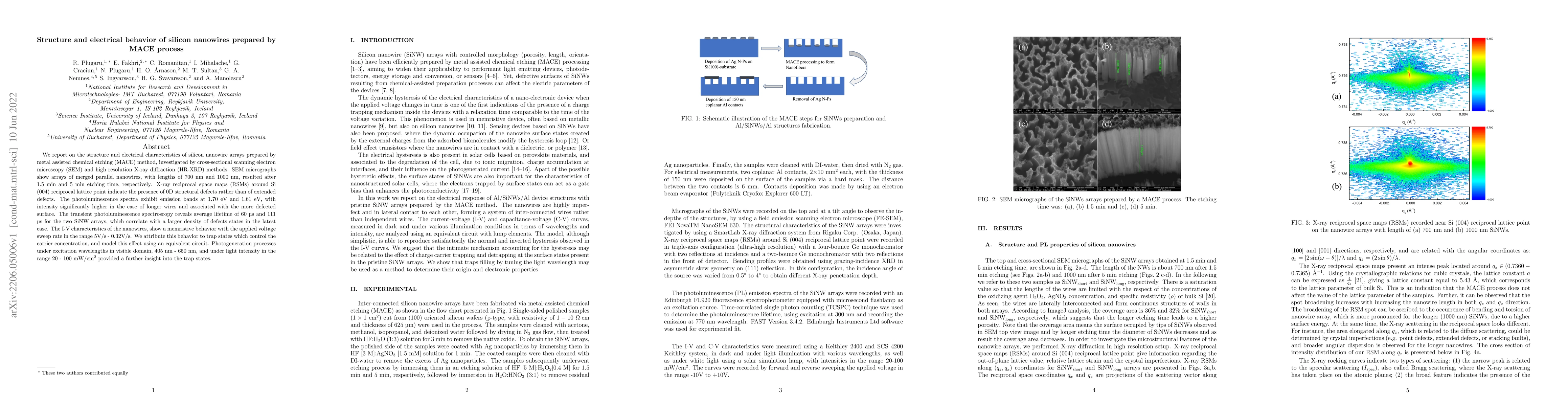
We report on the structure and electrical characteristics of silicon nanowire arrays prepared by metal assisted chemical etching (MACE) method, investigated by cross-sectional scanning electron microscopy (SEM) and high resolution X-ray diffraction (HR-XRD) methods. SEM micrographs show arrays of merged parallel nanowires, with lengths of 700 nm and 1000 nm, resulted after 1.5 min and 5 min etching time, respectively. X-ray reciprocal space maps (RSMs) around Si (004) reciprocal lattice point indicate the presence of 0D structural defects rather than of extended defects. The photoluminescence spectra exhibit emission bands at 1.70 eV and 1.61 eV, with intensity significantly higher in the case of longer wires and associated with the more defected surface. The transient photoluminescence spectroscopy reveals average lifetime of 60 $\mu$s and 111 $\mu$s for the two SiNW arrays, which correlate with a larger density of defects states in the latest case. The I-V characteristics of the nanowires, show a memristive behavior with the applied voltage sweep rate in the range 5V/s - 0.32V/s. We attribute this behavior to trap states which control the carrier concentration, and model this effect using an equivalent circuit. Photogeneration processes under excitation wavelengths in visible domain, 405 nm - 650 nm, and under light intensity in the range 20 - 100 mW/cm$^2$ provided a further insight into the trap states.
AI Key Findings
Get AI-generated insights about this paper's methodology, results, significance, and more — seven facets brought into focus.
Impact
Paper Details
Authors
PDF Preview
Key Terms
Citation Network
Current paper (gray), citations (green), references (blue)
Display is limited for performance on very large graphs.
Discussion 0