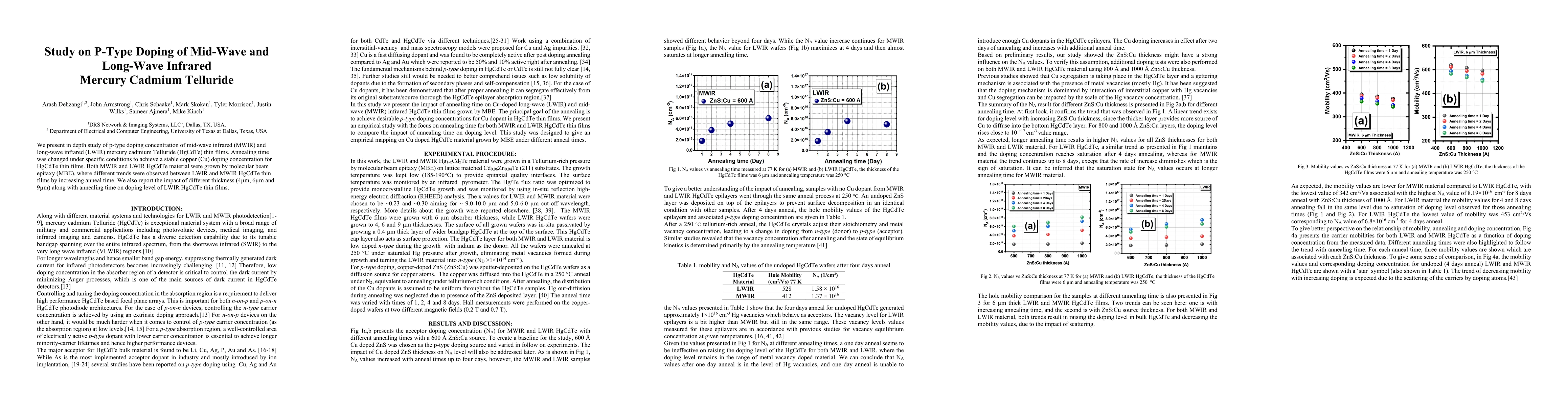
Comparative Study on Planar Type-II Strained-Layer Superlattice Infrared Photodetectors Fabricated by Ion-Implantation
|
A. Dehzangi
|
2022
|
View Paper
|
Band-structure-engineered high-gain LWIR photodetector based on a type-II superlattice
|
A. Dehzangi, Jiakai Li, M. Razeghi
|
2021
|
View Paper
|
Planar nBn type-II superlattice mid-wavelength infrared photodetectors using zinc ion-implantation
|
A. Dehzangi, Donghai Wu, R. Mcclintock, Jiakai Li, M. Razeghi
|
2020
|
View Paper
|
Advances in III-V semiconductor infrared absorbers and detectors
|
D. Ting, A. Soibel, A. Khoshakhlagh, S. Keo, Sir Rafol, A. Fisher, B. Pepper, E. Luong, C. Hill, S. Gunapala
|
2019
|
View Paper
|
High quantum efficiency mid-wavelength infrared type-II InAs/InAs1−xSbx superlattice photodiodes grown by metal-organic chemical vapor deposition
|
Donghai Wu, Q. Durlin, A. Dehzangi, Yiyun Zhang, M. Razeghi
|
2019
|
View Paper
|
High frequency response of LWIR HgCdTe photodiodes operated under zero-bias mode
|
M. Kopytko, P. Martyniuk, P. Madejczyk, K. Jóźwikowski, J. Rutkowski
|
2017
|
View Paper
|
Analog/RF Study of Self-aligned In0.53Ga0.47As MOSFET
with Scaled Gate Length
|
A. Dehzangi, F. Larki, M. F. Mohd Razip Wee, N. Wichmann, B. Majlis, S. Bollaert
|
2017
|
View Paper
|
High performance bias-selectable three-color Short-wave/Mid-wave/Long-wave Infrared Photodetectors based on Type-II InAs/GaSb/AlSb superlattices
|
A. Hoang, A. Dehzangi, S. Adhikary, M. Razeghi
|
2016
|
View Paper
|
Development of MBE HgCdTe for HDVIP® Focal-Plane Arrays
|
C. Schaake, R. Strong, M. Kinch, F. Harris, L. Robertson, Jun Zhao, F. Aqariden
|
2015
|
View Paper
|
HgCdTe: Recent Trends in the Ultimate IR Semiconductor
|
M. Kinch
|
2010
|
View Paper
|
Modeling of Copper SIMS Profiles in Thin HgCdTe
|
H. Schaake, M. Kinch, F. Aqariden
|
2008
|
View Paper
|
Bias dependent dual band response from InAs∕Ga(In)Sb type II strain layer superlattice detectors
|
A. Khoshakhlagh, J. B. Rodriguez, E. Plis, G. Bishop, Y. Sharma, H. Kim, L. Dawson, S. Krishna
|
2007
|
View Paper
|
Fundamentals of Infrared Detector Materials
|
M. Kinch
|
2007
|
View Paper
|
Development of Molecular Beam Epitaxially Grown Hg1−xCdxTe for High-Density Vertically-Integrated Photodiode-Based Focal Plane Arrays
|
F. Aqariden, P. Dreiske, M. Kinch, P. Liao, T. Murphy, H. Schaake, T. Shafer, H. Shih, T. Teherani
|
2007
|
View Paper
|
Bispectral thermal imaging with quantum-well infrared photodetectors and InAs/GaSb type-II superlattices
|
R. Rehm, M. Walther, J. Fleissner, J. Schmitz, J. Ziegler, W. Cabanski, R. Breiter
|
2006
|
View Paper
|
Two-color focal plane arrays based on self assembled quantum dots in a well heterostructure
|
S. Krishna, D. Forman, S. Annamalai, P. Dowd, P. Varangis, T. Tumolillo, A. Gray, J. Zilko, K. Sun, Mingguo Liu, J. Campbell, D. Carothers
|
2006
|
View Paper
|
Overcoming the doping bottleneck in semiconductors
|
Suhuai Wei
|
2004
|
View Paper
|
Mid-wavelength infrared p-on-n Hg1−xCdxTe heterostructure detectors: 30–120 kelvin state-of-the-Art performance
|
M. Zandian, J. Garnett, R. Dewames, M. Carmody, J. Pasko, M. Farris, C. Cabelli, D. Cooper, G. Hildebrandt, J. Chow, J. Arias, K. Vural, D. Hall
|
2003
|
View Paper
|
Chemical trends of defect formation and doping limit in II-VI semiconductors: The case of CdTe
|
Suhuai Wei, Shengbai Zhang
|
2002
|
View Paper
|
Fundamental studies on compensation mechanisms in II-VI compounds
|
Y. Marfaing
|
1996
|
View Paper
|
Properties of Narrow-Gap Cadmium-Based Compounds
|
P. Capper
|
1995
|
View Paper
|
Improvement in HgCdTe diode characteristics by low temperature post-implantation annealing
|
A. Ajisawa, N. Oda
|
1995
|
View Paper
|
Dopant diffusion in HgCdTe grown by photon assisted molecular‐beam epitaxy
|
T. Myers, K. Harris, R. Yanka, L. Mohnkern, R. J. Williams, G. Dudoff
|
1992
|
View Paper
|
Arsenic diffusion effects in CdxHg1-xTe layers grown by metal-organic vapour phase epitaxy
|
C. Maxey, P. Capper, P. Whiffin, B. C. Easton, I. Gale, J. Clegg, A. Harker
|
1989
|
View Paper
|
Influence of stoichiometry on the electrical activity of impurities in Hg(1−x)Cd(x)Te
|
P. Capper, J. Roberts, I. Kenworthy, C. L. Jones, J. Gosney, C. Ard, W. Coates
|
1988
|
View Paper
|
Group V acceptor doping of CdxHg1−xTe layers grown by metal-organic vapour phase epitaxy
|
P. Capper, P. Whiffin, B. C. Easton, C. Maxey, I. Kenworthy
|
1988
|
View Paper
|
Precipitation of tellurium in (Hg, Cd)Te alloys
|
H. Schaake, J. H. Tregilgas
|
1983
|
View Paper
|
Lattice defects in (Hg,Cd)Te: Investigations of their nature and evolution
|
H. Schaake, J. Tregilgas, A. Lewis, P. Everett
|
1983
|
View Paper
|
Effects of annealing on the electrical properties of Cd/x/Hg/1-x/Te
|
C. L. Jones, M. Quelch, P. Capper, J. Gosney
|
1982
|
View Paper
|
Lattice Defects in Semiconducting Hg1 − x Cd x Te Alloys II . Defect Structure of Indium‐Doped
|
H. Vydyanath
|
1981
|
View Paper
|
Copper impurity behaviour in CdTe films
|
E. Kučys, J. Jerhot, K. Bertulis, V. Bariss
|
1980
|
View Paper
|
Identification and investigation of impurities in undoped Hg1−xCdxTe
|
Jacob W. Lin
|
1975
|
View Paper
|
7 - HgCdTe photodetectors
|
|
2020
|
|
PHYSICS: A
|
|
2005
|
View Paper
|
Electrical doping of HgCdTe by ion implantation and heat treatment
|
G. Destefanis
|
1988
|
View Paper
|
Type conversion of (Hg,Cd)Te induced by the redistribution of residual acceptor impurities
|
J. Tregilgas, J. Beck, B. Gnade
|
1985
|
View Paper
|
Doping properties of selected impurities in Hg1−x Cdx Te
|
E. Johnson, J. Schmit
|
1977
|
View Paper
|
Phase equilibria and semiconducting properties of cadmium telluride
|
|
1958
|
|
Comments (0)