Sub-Atomic Channeling and Vortex Beams in SrTiO$_3$
Publication
Metrics
AI Quick Summary
Researchers studied electron probe propagation in SrTiO3 at sub-atomic length scales, discovering channeling and vortex beams that can be controlled by STEM parameters and temperature.
Paper Preview
Abstract
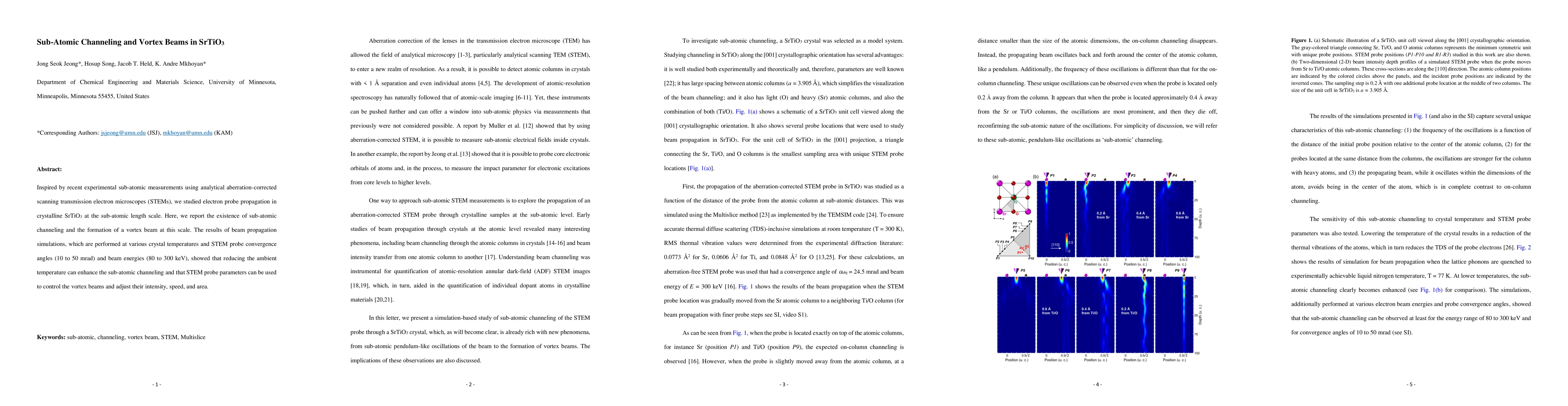
Inspired by recent experimental sub-atomic measurements using analytical aberration-corrected scanning transmission electron microscopes (STEMs), we studied electron probe propagation in crystalline SrTiO$_3$ at the sub-atomic length scale. Here, we report the existence of sub-atomic channeling and the formation of a vortex beam at this scale. The results of beam propagation simulations, which are performed at various crystal temperatures and STEM probe convergence angles (10 to 50 mrad) and beam energies (80 to 300 keV), showed that reducing the ambient temperature can enhance the sub-atomic channeling and that STEM probe parameters can be used to control the vortex beams and adjust their intensity, speed, and area.
AI Key Findings
Get AI-generated insights about this paper's methodology, results, significance, and more — seven facets brought into focus.
Impact
Paper Details
PDF Preview
Key Terms
Citation Network
Current paper (gray), citations (green), references (blue)
Display is limited for performance on very large graphs.
Discussion 0