Publication
Metrics
Paper Preview
Abstract
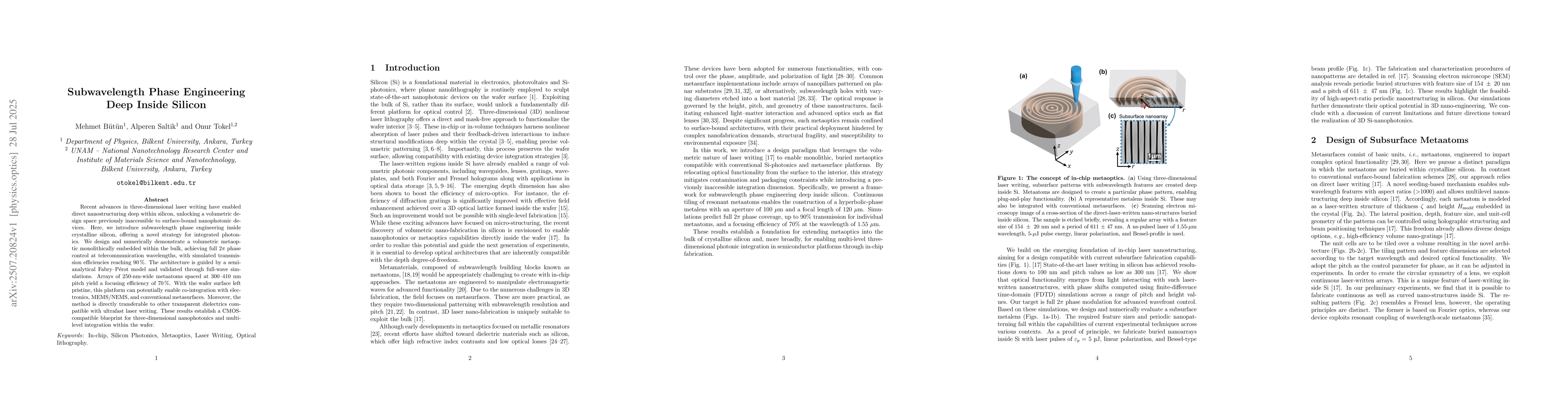
Recent advances in three-dimensional laser writing have enabled direct nanostructuring deep within silicon, unlocking a volumetric design space previously inaccessible to surface-bound nanophotonic devices. Here, we introduce subwavelength phase engineering inside crystalline silicon, offering a novel strategy for integrated photonics. We design and numerically demonstrate a volumetric metaoptic monolithically embedded within the bulk, achieving full 2$\pi$ phase control at telecommunication wavelengths, with simulated transmission efficiencies reaching 90 %. The architecture is guided by a semi-analytical Fabry-Perot model and validated through full-wave simulations. Arrays of 250-nm-wide metaatoms spaced at 300-410 nm pitch yield a focusing efficiency of 70 %. With the wafer surface left pristine, this platform can potentially enable co-integration with electronics, MEMS/NEMS, and conventional metasurfaces. Moreover, the method is directly transferable to other transparent dielectrics compatible with ultrafast laser writing. These results establish a CMOS-compatible blueprint for three-dimensional nanophotonics and multi-level integration within the wafer.
AI Key Findings
Get AI-generated insights about this paper's methodology, results, significance, and more — seven facets brought into focus.
Impact
Authors
PDF Preview
Citation Network
Current paper (gray), citations (green), references (blue)
Display is limited for performance on very large graphs.
Discussion 0