Super-compact universal quantum logic gates with inversedesigned elements
Publication
Metrics
AI Quick Summary
This paper reports the development of super-compact universal quantum logic gates using inverse design on silicon chips, achieving nearly vacuum wavelength dimensions for controlled-NOT and Hadamard gates, which are the smallest optical quantum gates to date. These compact gates enable the creation of significantly smaller quantum photonic circuits, paving the way for large-scale quantum information processing on chips.
Paper Preview
Abstract
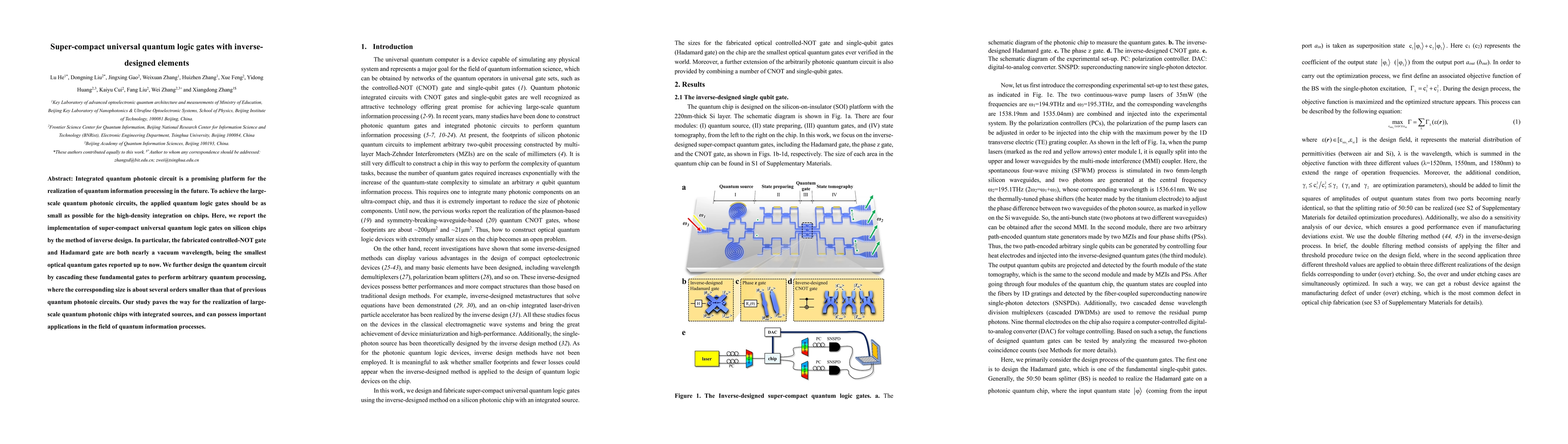
Integrated quantum photonic circuit is a promising platform for the realization of quantum information processing in the future. To achieve the largescale quantum photonic circuits, the applied quantum logic gates should be as small as possible for the high-density integration on chips. Here, we report the implementation of super-compact universal quantum logic gates on silicon chips by the method of inverse design. In particular, the fabricated controlled-NOT gate and Hadamard gate are both nearly a vacuum wavelength, being the smallest optical quantum gates reported up to now. We further design the quantum circuit by cascading these fundamental gates to perform arbitrary quantum processing, where the corresponding size is about several orders smaller than that of previous quantum photonic circuits. Our study paves the way for the realization of largescale quantum photonic chips with integrated sources, and can possess important applications in the field of quantum information processes.
AI Key Findings
Get AI-generated insights about this paper's methodology, results, significance, and more — seven facets brought into focus.
Impact
Paper Details
Authors
PDF Preview
Key Terms
Citation Network
Current paper (gray), citations (green), references (blue)
Display is limited for performance on very large graphs.
Discussion 0