Super-Resolution Nanolithography of Two-Dimensional Materials by Anisotropic Etching
Publication
Metrics
AI Quick Summary
This paper explores the use of anisotropic etching with sulfur hexafluoride (SF6) to improve the resolution and edge quality of nanostructures in various 2D materials, achieving smooth edges and sharp corners below the lithography resolution limit. The study demonstrates the technique's effectiveness on materials like hexagonal boron nitride and transition metal dichalcogenides, highlighting the anisotropic etching's potential for creating sub-10 nm features.
Paper Preview
Abstract
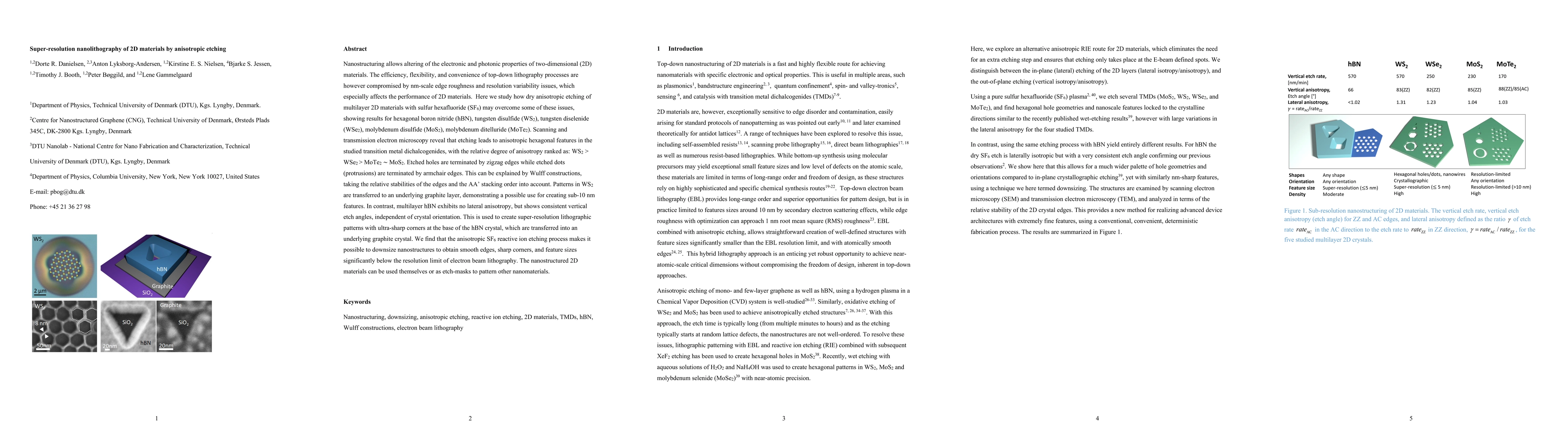
Nanostructuring allows altering of the electronic and photonic properties of two-dimensional (2D) materials. The efficiency, flexibility, and convenience of top-down lithography processes are however compromised by nm-scale edge roughness and resolution variability issues, which especially affects the performance of 2D materials. Here we study how dry anisotropic etching of multilayer 2D materials with sulfur hexafluoride (SF6) may overcome some of these issues, showing results for hexagonal boron nitride (hBN), tungsten disulfide (WS2), tungsten diselenide (WSe2), molybdenum disulfide (MoS2), molybdenum ditelluride (MoTe2). Scanning and transmission electron microscopy reveal that etching leads to anisotropic hexagonal features in the studied transition metal dichalcogenides, with the relative degree of anisotropy ranked as: WS2 > WSe2 > MoTe2 / MoS2. Etched holes are terminated by zigzag edges while etched dots (protrusions) are terminated by armchair edges. This can be explained by Wulff constructions, taking the relative stabilities of the edges and the AA stacking order into account. Patterns in WS2 are transferred to an underlying graphite layer, demonstrating a possible use for creating sub-10 nm features. In contrast, multilayer hBN exhibits no lateral anisotropy, but shows consistent vertical etch angles, independent of crystal orientation. This is used to create super-resolution lithographic patterns with ultra-sharp corners at the base of the hBN crystal, which are transferred into an underlying graphite crystal. We find that the anisotropic SF6 reactive ion etching process makes it possible to downsize nanostructures to obtain smooth edges, sharp corners, and feature sizes significantly below the resolution limit of electron beam lithography. The nanostructured 2D materials can be used themselves or as etch-masks to pattern other nanomaterials.
AI Key Findings
Get AI-generated insights about this paper's methodology, results, significance, and more — seven facets brought into focus.
Impact
Paper Details
Authors
PDF Preview
Key Terms
Citation Network
Current paper (gray), citations (green), references (blue)
Display is limited for performance on very large graphs.
Discussion 0