Summary
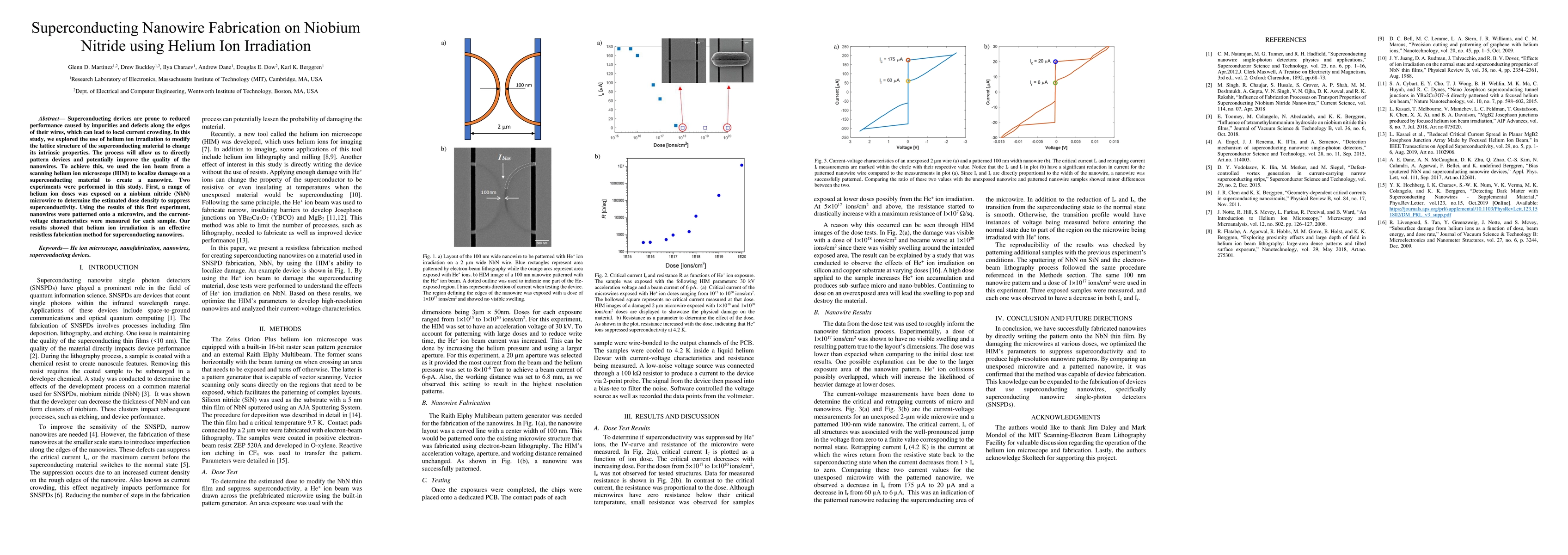
Superconducting devices are prone to reduced performance caused by impurities and defects along the edges of their wires, which can lead to local current crowding. In this study, we explored the use of helium ion irradiation to modify the lattice structure of the superconducting material to change its intrinsic properties. The process will allow us to directly pattern devices and potentially improve the quality of the nanowires. To achieve this, we used the ion beam from a scanning helium ion microscope (HIM) to localize damage on a superconducting material to create a nanowire. Two experiments were performed in this study. First, a range of helium ion doses was exposed on a niobium nitride (NbN) microwire to determine the estimated dose density to suppress superconductivity. Using the results of this first experiment, nanowires were patterned onto a microwire, and the current-voltage characteristics were measured for each sample. Our results showed that helium ion irradiation is an effective resistless fabrication method for superconducting nanowires.
AI Key Findings
Get AI-generated insights about this paper's methodology, results, and significance.
Paper Details
PDF Preview
Key Terms
Citation Network
Current paper (gray), citations (green), references (blue)
Display is limited for performance on very large graphs.
Similar Papers
Found 4 papersSite-Selective Enhancement of Superconducting Nanowire Single-Photon Detectors via Local Helium Ion Irradiation
Kai Müller, Rudolf Gross, Jonathan J. Finley et al.
Impact of helium ion irradiation on the thermal properties of superconducting nanowire single-photon detectors
Hao Li, Zhen Wang, Xin Ou et al.
Effect of ion irradiation on superconducting thin films
Katja Kohopää, Alberto Ronzani, Robab Najafi Jabdaraghi et al.
| Title | Authors | Year | Actions |
|---|

Comments (0)